|
|


 Arabic
 Bengali
 Chinese
 English
 French
 German
 Hebrew
 Hindi
Hindi Italian
 Japanese
 Korean
 Malay
Malay Polish
 Portuguese
 Spanish
 Turkish
 Ukrainian
 Vietnamese
|
ENCYCLOPEDIA OF RADIO ELECTRONICS AND ELECTRICAL ENGINEERING Voltage stabilizer with protection against short circuit and overcurrent, 14-20/12 volts 0,5 amps. Encyclopedia of radio electronics and electrical engineering
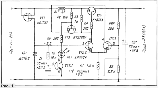
Encyclopedia of radio electronics and electrical engineering / Surge Protectors The author analyzes the most characteristic features and shortcomings of voltage stabilizers, familiar to radio amateurs from publications in our magazine, gives practical advice, sometimes unconventional, to improve their main parameters. As an example, he talks about the stabilizer he developed, intended for powerful power supplies for equipment that operates around the clock. The article describes the manufacturing technology of the heat sink of a powerful transistor. Network power supplies, in which radio amateurs use microcircuit stabilizers to stabilize the rectified voltage, do not always please their creators. The reason for this is the inherent disadvantages of these designs. Traditional transistor regulators often have unreliable overload protection. Inertialess protection systems falsely operate even from short-term overloads when connecting a capacitive load. Inertial protection means do not have time to work with a strong current pulse, for example, during a short circuit, leading to a breakdown of transistors [1]. Devices with an output current limiter are inertialess, they have no trigger effect, but in the event of a short circuit, a large power is dissipated on the control transistor, which requires the use of an appropriate heat sink [2]. The only way out in such a situation is the simultaneous use of means for limiting the output current and inertial protection of the control transistor from overload, which will provide it with two to three times less power and dimensions of the heat sink. But this leads to an increase in the number of elements, dimensions of the structure and complicates the repeatability of the device in amateur conditions. A schematic diagram of the stabilizer, the number of elements in which is minimal, is shown in fig. 1.
The source of exemplary voltage is a thermally stabilized zener diode VD1. To exclude the influence of the input voltage of the stabilizer on the mode of the zener diode, its current is set by a stable current generator (GST) built on a field-effect transistor VT1. Thermal stabilization and stabilization of the current of the zener diode increase the coefficient of stabilization of the output voltage. The exemplary voltage is supplied to the left (according to the circuit) input of the differential amplifier on transistors VT2.2 and VT2.3 of the K125NT1 microassembly and resistor R7, where it is compared with the feedback voltage taken from the output voltage divider R8R9. The voltage difference at the inputs of a differential amplifier changes the balance of the collector currents of its transistors. The regulating transistor VT4, controlled by the collector current of the transistor VT2.2, has a large base current transfer coefficient. This increases the depth of feedback and increases the stabilization factor of the device, and also reduces the power dissipated by the differential amplifier transistors. Let's consider the operation of the device in more detail. Let's assume that in the steady state, with an increase in the load current, the output voltage will decrease slightly, which will also cause a decrease in the voltage at the emitter junction of the transistor VT3.2. In this case, the collector current will also decrease. This will increase the current of the transistor VT2.2, since the sum of the output currents of the transistors of the differential amplifier is equal to the current flowing through the resistor R7, and practically does not depend on the mode of operation of its transistors. In turn, the growing current of the transistor VT2.2 causes an increase in the collector current of the regulating transistor VT4, proportional to its base current transfer coefficient, increasing the output voltage to its original level and allowing it to be maintained unchanged regardless of the load outflow. For short-term protection of the device with its return to its original state, a collector current limiter of the regulating transistor is introduced, made on the transistor VT3 and resistors R1, R2. Resistor R1 performs the function of a current sensor flowing through the regulating transistor VT4. If the current of this transistor exceeds the maximum value (about 0,5 A), the voltage drop across the resistor R1 will reach 0,6 V, i.e., the threshold voltage for opening the transistor VT3. Opening, it shunts the emitter junction of the regulating transistor, thereby limiting its current to about 0,5 A. Thus, when the load current exceeds the maximum value for a short time, the transistors VT3 and VT4 operate in the HTS mode, which causes a drop in the output voltage without triggering the overcurrent protection. After some time, proportional to the time constant of the R5C1 circuit, this leads to the opening of the transistor VT2.1 and the further opening of the transistor VT3, which closes the transistor VT4. This state of the transistors is stable, therefore, after eliminating the short circuit or de-energizing the load, it is necessary to disconnect the device from the network and turn it on again after discharging the capacitor C1. The short-circuit current of the device is zero, which means that it excludes overheating of the control transistor when the protection is triggered. Resistor R3 is necessary for the reliable operation of the transistor VT4 at low currents and elevated temperatures. Capacitor C2, shunting the output of the stabilizer, prevents self-excitation of the device, which can be caused by deep OOS in voltage. Resistor R6 in the collector circuit of the transistor VT2.1 limits the current during transients when the protection is turned on, and the HL1 LED acts as an overload indicator. Main parameters of the stabilizer
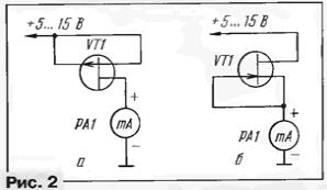
The stabilizer is not critical to the layout of the printed circuit board and the placement of parts on it. Therefore, its installation depends mainly on the experience of the designer himself and the dimensions of the pre-selected parts. The field effect transistor VT1 should be selected so that the stabilization current, measured according to the circuit in Fig. 2, a or 2, b, was within 5 ... 15 mA. The static current transfer coefficient of the base of the transistor VT3 must be at least 20, and the transistor VT4 - at least 400. On the regulating transistor VT4, the allowable collector current of which must be at least 1 A, significant power is released, so it should be installed on a heat sink with a power of about 5 Tue
Resistors and capacitors - any types for the ratings indicated on the diagram. Starting to test and adjust the stabilizer, the resistor R5 is temporarily removed so that the protection system does not work, and by selecting the resistor R8, the output voltage is set to 12 V. After that, the resistor R5 is turned on and the required value of the tripping current of the device protection by current is achieved by selecting the resistor R1. What changes or additions can be made to the recommended stabilizer? If the radio amateur does not have a suitable field-effect transistor, the DC generator can be assembled on a bipolar transistor KT3108A (Fig. 3, a) or similar from the KT361 series with a base current transfer coefficient of at least 20. Diodes VD3 and VD4 can be any silicon.
The thermally stabilized zener diode D818V (VD1) can be replaced with any other similar one for stabilization voltage from 3 to 12 V. But the most desirable is a two-anode zener diode, for example KS162A, with a low temperature coefficient of stabilization voltage. In the extreme case, it will be replaced by a chain of conventional zener diodes connected in series and any silicon diode, as shown in Fig. 3b. The regulating transistor KT825A (VT4) can be replaced by two by turning them on according to the composite transistor circuit, as shown in fig. 4a or 4b. Transistor VT4' must be with a current gain of at least 20, a maximum collector current of at least 1 A and a maximum power dissipation with a heat sink of at least 5 W. Transistor VT4 "- any p-n-p structure with a current gain of at least 20, a maximum collector current of at least 30 mA and a maximum dissipated power of at least 150 mW, for example, the KT361, KT203, KT208, KT209, KT501, KT502 series .
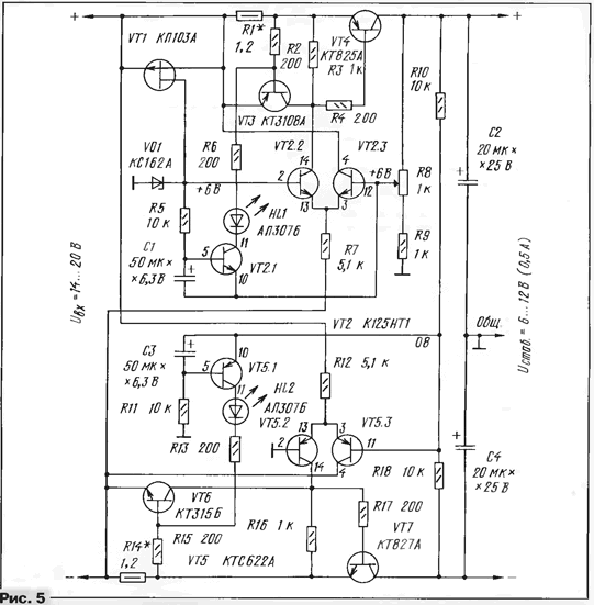
To reduce the saturation voltage of the transistor VT4 "and, as a result, some decrease in the dissipated power, it is advisable to make the composite transistor according to the scheme of Fig. 4, c. In this case, the power dissipated by the transistor VT4" will increase to 0,6 W. Suitable transistors of the KT814, KT816, GT402 series or others with similar parameters. Transistors VT2.2 and VT2.3 of the K125NT1 microassembly operating in a differential stage can be replaced with an assembly of two p-pn transistors with a current gain of at least 20, a maximum collector-emitter voltage of at least 20 V and a collector current of at least 15 mA, for example, the KP198 series. In this case, it is only important to remember: the same current-voltage characteristics of both transistors of the differential stage are necessary to ensure that the voltage taken from the divider R8R9 is equal to the exemplary one, which guarantees the independence of the output voltage of the stabilizer from the load current. If such equality is not required, then these microassembly elements can be replaced by any low-power p-pn transistors with similar parameters. In this case, and also if the microassembly consists of only two elements, the function of the VT2.1 transistor can be performed by a similar low-power n-p-n transistor. The described stabilizer with a fixed output voltage can be easily converted into a bipolar one with an adjustable output voltage from ±6 V to ±12 V. A diagram of such a device is shown in fig. 5.
The stabilization voltage limits can be expanded by replacing the KS162A (VD1) zener diode with KS147A and reducing the resistance of the resistor R9 to 330 ohms. It is also possible to mount the differential amplifier and voltage divider R8R9 according to the scheme of fig. 6.
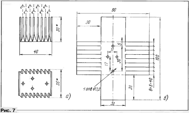
Then the output voltage of the stabilizer can be changed from 0 to ±12 V. However, the protection system, which includes elements VT2.1, R5, C1, HL1 (Fig. 1), in this case will lose its meaning and the stabilizer will become quite traditional. Transistors VT1, VT2 and VT4, the values of resistors and capacitors are the same as in the stabilizer according to the circuit in fig. 1, but the dissipation power of the transistor VT4 (or transistors VT4 ', VT4 "according to the diagrams in Fig. 4) will increase in proportion to the voltage drop across it. Heat sinks of powerful transistors of the KT825 or KT827 series, which act as regulators, can be self-made. A possible design of one of these heat sinks is shown in Fig. 7a. The blank for it (Fig. 7, b) is cut out with scissors for metal or cut out with a jigsaw from sheet aluminum 2 mm thick. Then the narrow petals of the opposite sides of the workpiece are turned with pliers by 90 ° around their own axis each, and the wide petals are bent (along the dashed lines) upwards.
Literature
Author: V.Kozlov, Murom, Vladimir Region
Artificial leather for touch emulation
15.04.2024 Petgugu Global cat litter
15.04.2024 The attractiveness of caring men
14.04.2024
▪ Adam II - a tablet with a two-sided display ▪ Colorless non-marking coffee ▪ Washing with almost no water ▪ Walking speed measurement without wearable devices ▪ Atypical volcanic activity noticed in Europe
▪ section of the site Personal transport: land, water, air. Article selection ▪ article What does the coming day prepare for me? Popular expression ▪ article Where is the island in the lake, the area exceeding the lake itself? Detailed answer ▪ article Tuberous capuchin. Legends, cultivation, methods of application ▪ article Double-chip filter for SSB. Encyclopedia of radio electronics and electrical engineering ▪ article Color reactions with glucose. Chemical experience
Home page | Library | Articles | Website map | Site Reviews
www.diagram.com.ua |


 Leave your comment on this article: