|
|


 Arabic
 Bengali
 Chinese
 English
 French
 German
 Hebrew
 Hindi
Hindi Italian
 Japanese
 Korean
 Malay
Malay Polish
 Portuguese
 Spanish
 Turkish
 Ukrainian
 Vietnamese
|
ENCYCLOPEDIA OF RADIO ELECTRONICS AND ELECTRICAL ENGINEERING Transformerless power supplies. Encyclopedia of radio electronics and electrical engineering
Encyclopedia of radio electronics and electrical engineering / Power Supplies Now the house has a lot of small-sized equipment that needs constant power. These are watches with LED indication, and thermometers, and small-sized receivers, etc. In principle, they are designed for batteries, but they "sit down" at the most inopportune moment. A simple way out is to power them from mains power supplies. But even a small-sized network (step-down) transformer is quite heavy and takes up not so little space, and switching power supplies are still complex, requiring certain experience and expensive equipment for manufacturing. The solution to this problem, under certain conditions, can be a transformerless power supply with a quenching capacitor. These conditions:
This is due to the fact that when powered by a transformerless unit, the device is under the potential of the network, and touching its non-isolated elements can “shake” well. It is worth adding that when setting up such power supplies, safety precautions and caution should be observed. If it is necessary to use an oscilloscope for adjustment, the power supply must be connected through an isolation transformer. In its simplest form, the transformerless power supply circuit has the form shown in Fig. 1.
To limit the inrush current when the unit is connected to the network, resistor R1 is connected in series with the capacitor C1 and the rectifier bridge VD2, and resistor R1 is connected in parallel to it to discharge the capacitor after disconnection. A transformerless power supply in the general case is a symbiosis of a rectifier and a parametric stabilizer. Capacitor C1 for alternating current is a capacitive (reactive, i.e. not consuming energy) resistance Xc, the value of which is determined by the formula:
where (- network frequency (50 Hz); C-capacitance of capacitor C1, F. Then the output current of the source can be approximately determined as follows:
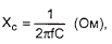
where Uc is the mains voltage (220 V). The input part of another power supply (Fig. 2a) contains a ballast capacitor C1 and a bridge rectifier made of diodes VD1, VD2 and zener diodes VD3, VD4. Resistors R1, R2 play the same role as in the first circuit. The output voltage waveform of the block is shown in Fig. 2b (when the output voltage exceeds the stabilization voltage of the zener diodes, otherwise it works like a normal diode).
From the beginning of the positive half-cycle of the current through the capacitor C1 until the moment t1, the zener diode VD3 and the diode, VD2 are open, and the zener diode VD4 and the diode VD1 are closed. In the time interval t1 ... t3, the zener diode VD3 and the diode VD2 remain open, and a stabilization current pulse passes through the opened zener diode VD4. The voltage at the output Uout and at the zener diode VD4 is equal to its stabilization voltage Ust. The stabilization pulse current, which is through for the diode-zener diode rectifier, bypasses the load RH, which is connected to the output of the bridge. At the moment t2, the stabilization current reaches its maximum, and at the moment t3 it is equal to zero. Until the end of the positive half-cycle, the zener diode VD3 and the diode VD2 remain open. At the moment t4, the positive half-cycle ends and the negative half-cycle begins, from the beginning of which until the moment t5 the zener diode VD4 and the diode VD1 are already open, and the zener diode VD3 and the diode VD2 are closed. In the time interval t5-t7, the zener diode VD4 and the diode VD1 continue to remain open, and through the zener diode VD3 at a voltage of UCT, a through stabilization current pulse passes, maximum at time t6. Starting from t7 and until the end of the negative half-cycle, the zener diode VD4 and the diode VD1 remain open. The considered cycle of operation of the diode-zener diode rectifier is repeated in the following periods of mains voltage. Thus, a rectified current passes through the zener diodes VD3, VD4 from the anode to the cathode, and in the opposite direction - a pulsed stabilization current. In the time intervals t1...t3 and t5...t7, the stabilization voltage changes by no more than a few percent. The value of the alternating current at the input of the bridge VD1 ... VD4 in the first approximation is equal to the ratio of the mains voltage to the capacitance of the ballast capacitor C1. The operation of a diode-zener diode rectifier without a ballast capacitor that limits the through current is impossible. In functional terms, they are inseparable and form a single whole - a capacitor-zener diode rectifier. The spread of UCT values of the same type of zener diodes is approximately 10%, which leads to the appearance of additional output voltage ripples with the mains frequency, the amplitude of the ripple voltage is proportional to the difference in the values of Ust of the zener diodes VD3 and VD4. When using powerful zener diodes D815A ... D817G, they can be installed on a common radiator if the letters “PP” are present in their type designation (zener diodes D815APP ... D817GPP have reverse polarity of the terminals). Otherwise, diodes and zener diodes must be swapped. Transformerless power supplies are usually assembled according to the classical scheme: a quenching capacitor, an AC voltage rectifier, a filter capacitor, a stabilizer. The capacitive filter smooths out the output voltage ripple. The larger the capacitance of the filter capacitors, the less ripple and, accordingly, the greater the constant component of the output voltage. However, in some cases, you can do without a filter, which is often the most cumbersome part of such a power source. It is known that a capacitor included in an alternating current circuit shifts its phase by 90 °. A phase-shifting capacitor is used, for example, when connecting a three-phase motor to a single-phase network. If a phase-shifting capacitor is used in the rectifier, which provides mutual overlapping of the half-waves of the rectified voltage, in many cases it is possible to do without a bulky capacitive filter or significantly reduce its capacitance. A diagram of such a stabilized rectifier is shown in Fig. 3.
A three-phase rectifier VD1.VD6 is connected to an AC voltage source through active (resistor R1) and capacitive (capacitor C1) resistance. The output voltage of the rectifier stabilizes the Zener diode VD7. Phase-shifting capacitor C1 must be designed for operation in AC circuits. Here, for example, capacitors of the K73-17 type with an operating voltage of at least 400 V are suitable. Such a rectifier can be used where it is necessary to reduce the dimensions of the electronic device, since the dimensions of the oxide capacitors of the capacitive filter are usually much larger than the phase-shifting capacitor of a relatively small capacity. Another advantage of the proposed option is that the consumed current is practically constant (in the case of a constant load), while in rectifiers with a capacitive filter at the moment of switching on, the starting current significantly exceeds the steady-state value (due to the charge of the filter capacitors), which in some cases is highly undesirable . The described device can also be used with series voltage stabilizers with a constant load, as well as with a load that does not require voltage stabilization. A completely simple transformerless power supply (Fig. 4) can be built "on the knee" in just half an hour.
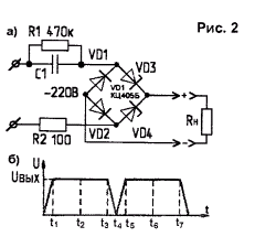
In this embodiment, the circuit is designed for an output voltage of 6,8 V and a current of 300 mA. The voltage can be changed by replacing the Zener diode VD4 and, if necessary, VD3. And by installing transistors on radiators, you can also increase the load current. Diode bridge - any, designed for a reverse voltage of at least 400 V. By the way, we can also recall the "ancient" diodes. D226B. In another transformerless source (Fig. 5), a KR142EN8 microcircuit is used as a stabilizer. Its output voltage is 12 V. If it is necessary to adjust the output voltage, then pin 2 of the DA1 chip is connected to the common wire through a variable resistor, for example, of the SPO-1 type (with a linear resistance change characteristic). Then the output voltage can vary in the range of 12...22 V. As a DA1 microcircuit, to obtain other output voltages, it is necessary to use the appropriate integrated stabilizers, for example, KR142EN5, KR1212EN5, KR1157EN5A, etc. Capacitor C1 must be required for an operating voltage of at least 300 V, brand K76-3, K73-17 or similar (non-polar , high voltage). Oxide capacitor C2 acts as a power filter and smooths out voltage ripples. Capacitor C3 reduces high frequency noise. Resistors R1, R2 - type MLT-0,25. Diodes VD1...VD4 can be replaced with KD105B...KD105G, KD103A, B, KD202E. The VD5 zener diode with a stabilization voltage of 22 ... 27 V protects the microcircuit from voltage surges at the moment the source is turned on.
Despite the fact that theoretically capacitors in an AC circuit do not consume power, in reality, some heat can be generated in them due to the presence of losses. You can check the suitability of the capacitor as a quenching capacitor for use in a transformerless source by simply connecting it to the mains and estimating the case temperature after half an hour. If the capacitor has time to noticeably warm up, it is not suitable. Special capacitors for industrial electrical installations practically do not heat up (they are designed for high reactive power). Such capacitors are commonly used in fluorescent lamps, in ballasts of asynchronous electric motors, etc. In a 5-volt source (Fig. 6) with a load current of up to 0,3 A, a capacitor voltage divider is used. It consists of a paper capacitor C1 and two oxide capacitors C2 and C3, which form the lower (according to the circuit) non-polar shoulder with a capacity of 100 μF (counter-series connection of capacitors). Bridge diodes serve as polarizing diodes for the oxide pair. With the indicated ratings of the elements, the short-circuit current at the output of the power supply is 600 mA, the voltage across the capacitor C4 in the absence of load is 27 V.
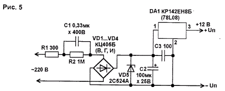
The power supply unit for the portable receiver (Fig. 7) fits easily into its battery compartment. The diode bridge VD1 is designed for operating current, its limiting voltage is determined by the voltage provided by the zener diode VD2. Elements R3, VD2. VT1 form an analogue of a powerful zener diode. The maximum current and power dissipation of such a zener diode are determined by the transistor VT1. It may require a heatsink. But in any case, the maximum current of this transistor should not be less than the load current. Elements R4, VD3 - a circuit for indicating the presence of an output voltage. At low load currents, the current consumed by this circuit must be taken into account. Resistor R5 loads the power circuit with a small current, which stabilizes its operation.
Quenching capacitors C1 and C2 - type KBG or similar. You can also use K73-17 with an operating voltage of 400 V (suitable with 250 V, since they are connected in series). The output voltage depends on the resistance of the quenching capacitors to alternating current, the actual load current and on the stabilization voltage of the zener diode. To stabilize the voltage of a transformerless power supply with a quenching capacitor, you can use symmetrical dinistors (Fig. 8).
When charging the filter capacitor C2 to the opening voltage of the dinistor VS1, it turns on and shunts the input of the diode bridge. The load at this time receives power from the capacitor C2 At the beginning of the next half-cycle, C2 is recharged again to the same voltage, and the process is repeated. The initial discharge voltage of the capacitor C2 does not depend on the load current and mains voltage, so the stability of the output voltage of the unit is quite high. The voltage drop across the dinistor in the on state is small, the power dissipation, and hence its heating, is much less than that of the zener diode. The maximum current through the dinistor is about 60 mA. If this value is not enough to obtain the required output current, you can “power up the dinistor with a triac or thyristor (Fig. 9). The disadvantage of such power supplies is the limited choice of output voltages, determined by the turn-on voltages of the dinistors.
A transformerless power supply with adjustable output voltage is shown in Fig. 10a.
Its peculiarity lies in the use of adjustable negative feedback from the output of the block to the transistor cascade VT1, connected in parallel with the output of the diode bridge. This cascade is a regulating element and is controlled by a signal from the output of a single-stage amplifier to VT2. The output signal VT2 depends on the voltage difference supplied from the variable resistor R7, connected in parallel to the output of the power supply, and the reference voltage source on the diodes VD3, VD4. Essentially, the circuit is an adjustable shunt regulator. The role of the ballast resistor is played by the quenching capacitor C1, the parallel controlled element is the transistor VT1. This power supply works as follows. When connected to the network, the transistors VT1 and VT2 are locked, and the storage capacitor C2 is charged through the diode VD2. When the base of the transistor VT2 reaches a voltage equal to the reference voltage on the diodes VD3, VD4, the transistors VT2 and VT1 are unlocked. Transistor VT1 shunts the output of the diode bridge, and its output voltage drops, which leads to a decrease in the voltage on the storage capacitor C2 and to the blocking of transistors VT2 and VT1. This, in turn, causes an increase in voltage on C2, unlocking VT2, VT1 and repeating the cycle. Due to the negative feedback acting in this way, the output voltage remains constant (stabilized) both with the load on (R9) and without it (at idle). Its value depends on the position of the R7 potentiometer slider. The upper (according to the diagram) position of the engine corresponds to a larger output voltage. The maximum output power of the above device is 2 watts. The output voltage adjustment limits are from 16 to 26 V, and with a shorted diode VD4 - from 15 to 19,5 V. The ripple level at the load is not more than 70 mV. Transistor VT1 operates in variable mode: in the presence of a load - in linear mode, at idle - in pulse-width modulation (PWM) mode with a voltage ripple frequency across capacitor C2 of 100 Hz. In this case, the voltage pulses on the collector VT1 have gentle fronts. The criterion for the correct choice of capacitance C1 is to obtain the required maximum voltage at the load. If its capacitance is reduced, then the maximum output voltage at the rated load is not reached. Another criterion for choosing C1 is the invariance of the voltage waveform at the output of the diode bridge (Fig. 10b).
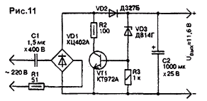
The voltage waveform has the form of a sequence of rectified sinusoidal half-waves of the mains voltage with limited (flattened) tops of positive half-sine waves, the amplitude of the tops is a variable, depending on the position of the R7 slider, and changes linearly with its rotation. But each half-wave must necessarily reach zero, the presence of a constant component (as shown in Fig. 10b by a dotted line) is not allowed, because in this case, the stabilization mode is violated. The linear mode is lightweight, the VT1 transistor heats up a little and can work with little or no heatsink. A slight heating takes place in the lower position of the R7 engine (at the minimum output voltage). At idle, the thermal regime of the transistor VT1 deteriorates in the upper position of the R7 engine. In this case, the transistor VT1 must be installed on a small radiator, for example, in the form of a "flag" made of a square-shaped aluminum plate with a side of 30 mm and a thickness of 1 ... 2 mm. Regulating transistor VT1 - medium power, with a high transfer coefficient. Its collector current must be 2 ... 3 times the maximum load current, the allowable collector-emitter voltage is not less than the maximum output voltage of the power supply. As VT1, transistors KT972A, KT829A, KT827A, etc. can be used. Transistor VT2 operates in low current mode, so any low-power pn-p transistor is suitable - KT203, KT361, etc. Resistors R1, R2 - protective. They protect the control transistor VT1 from failure due to overcurrent during transients at the time the unit is connected to the network. The transformerless capacitor rectifier (Fig. 11) operates with auto-stabilization of the output voltage. This is achieved by changing the connection time of the diode bridge to the storage capacitor. Parallel to the output of the diode bridge, the transistor VT1 is connected, operating in the key mode. The base VT1 is connected through a zener diode VD3 to a storage capacitor C2, separated by a direct current from the output of the bridge by a diode VD2 to prevent rapid discharge when VT1 is open. As long as the voltage on C2 is less than the stabilization voltage VD3, the rectifier works as usual. When the voltage on C2 increases and VD3 opens, the transistor VT1 also opens and shunts the output of the rectifier bridge. The voltage at the output of the bridge abruptly decreases to almost zero, which leads to a decrease in the voltage on C2 and turning off the zener diode and the switching transistor.
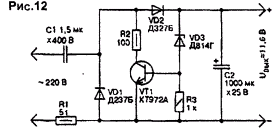
Further, the voltage on the capacitor C2 increases again until the zener diode and transistor are turned on, etc. The process of auto-stabilization of the output voltage is very similar to the operation of a switching voltage regulator with pulse-width regulation. Only in the proposed device, the pulse repetition rate is equal to the voltage ripple frequency on C2. To reduce losses, the key transistor VT1 must be with a high gain, for example, KT972A, KT829A, KT827A, etc. You can increase the output voltage of the rectifier by using a higher voltage zener diode (low-voltage chain connected in series). With two zener diodes D814V, D814D and a capacitance of capacitor C1 of 2 μF, the output voltage at a load with a resistance of 250 ohms can be 23 ... 24 V. Similarly, you can stabilize the output voltage of a half-wave diode-capacitor rectifier (Fig. 12).
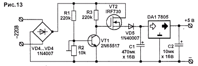
For a rectifier with a positive output voltage, an npn transistor is connected in parallel with the diode VD1, controlled from the output of the rectifier through the zener diode VD3. When the capacitor C2 reaches a voltage corresponding to the moment the zener diode opens, the transistor VT1 also opens. As a result, the amplitude of the positive half-wave of the voltage supplied to C2 through the VD2 diode decreases almost to zero. When the voltage on C2 decreases, the transistor VT1 closes due to the zener diode, which leads to an increase in the output voltage. The process is accompanied by pulse-width regulation of the pulse duration at the input VD2, therefore, the voltage across the capacitor C2 is stabilized. In a rectifier with a negative output voltage, a pnp transistor KT1A or KT973A must be connected in parallel with the VD825 diode. The output stabilized voltage at a load with a resistance of 470 ohms is about 11 V, the ripple voltage is 0,3 ... 0,4 V. In both versions, the zener diode operates in a pulsed mode at a current of a few milliamps, which is in no way related to the rectifier load current, the quenching capacitor capacitance spread, and mains voltage fluctuations. Therefore, the losses in it are significantly reduced, and it does not require heat removal. The key transistor also does not require a radiator. Resistors R1, R2 in these circuits limit the input current during transients at the moment the device is connected to the network. Due to the inevitable "bounce" of the contacts of the mains plug, the switching process is accompanied by a series of short circuits and circuit breaks. With one of these short circuits, the quenching capacitor C1 can charge up to the full amplitude value of the mains voltage, i.e. up to about 300 V. After a break and subsequent short circuit due to "bounce", this and the mains voltage can add up to a total of about 600 V. This is the worst case that must be taken into account to ensure reliable operation of the device. Another version of the key transformerless power supply circuit is shown in Fig. 13.
The mains voltage, passing through the diode bridge on VD1.VD4, is converted into a pulsating amplitude of about 300 V. Transistor VT1 is a comparator, VT2 is a key. Resistors R1, R2 form a voltage divider for VT1. By adjusting R2, you can set the comparator response voltage. Until the voltage at the output of the diode bridge reaches the set threshold, the transistor VT1 is closed, the gate VT2 has a trigger voltage and it is open. Capacitor C2 is charged through VT5 and diode VD1. When the set threshold is reached, the transistor VT1 opens and shunts the gate VT2. The key closes and opens again when the voltage at the output of the bridge becomes less than the threshold of the comparator. Thus, a voltage is set on C1, which is stabilized by the integral stabilizer DA1. With the ratings shown in the diagram, the source provides an output voltage of 5 V at a current of up to 100 mA. The setting consists in setting the threshold VT1. Instead of IRF730 can be used. KP752A, IRF720, BUZ60, 2N6517 is replaced by KT504A. A miniature transformerless power supply for low-power devices can be built on the HV-2405E chip (Fig. 14), which directly converts AC to DC.
The input voltage range of the IC is -15 ... 275 V. The output voltage range is 5 ... 24 V at a maximum output current of up to 50 mA. Available in a flat plastic DIP-8 package. The structure of the microcircuit is shown in Fig. 15a, the pinout is shown in Fig. 15b.
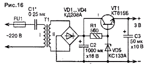
In the source circuit (Fig. 14), special attention should be paid to the resistors R1 and R2. Their total resistance should be around 150 ohms, and the power dissipation should be at least 3 watts. The input high voltage capacitor C1 can have a capacitance from 0,033 to 0,1 uF. Almost any varistor Rv can be used with an operating voltage of 230.250 V. Resistor R3 is selected depending on the required output voltage. In its absence (outputs 5 and 6 are closed), the output voltage is slightly more than 5 V, with a resistance of 20 kOhm, the output voltage is about 23 V. Instead of a resistor, you can turn on a zener diode with the necessary stabilization voltage (from 5 to 21 V). There are no special requirements for the rest of the details, with the exception of the choice of the operating voltage of electrolytic capacitors (the formulas for calculation are shown in the diagram). Given the potential danger of transformerless sources, in some cases a compromise option may be of interest: with a quenching capacitor and a transformer (Fig. 16).
A transformer with a high-voltage secondary winding is suitable here, since the required rectified voltage is set by selecting the capacitance of capacitor C1. The main thing is that the transformer windings provide the required current. To prevent the device from failing when the load is disconnected, a D1P zener diode should be connected to the output of the VD4 ... VD815 bridge. In normal mode, it does not work, because its stabilization voltage is higher than the working one at the output of the bridge. Fuse FU1 protects the transformer and stabilizer in the event of a breakdown of capacitor C1. In sources of this type, in a circuit of series-connected capacitive (capacitor C1) and inductive (transformer T1) resistances, voltage resonance may occur. This should be remembered when adjusting them and control the voltage with an oscilloscope. Author: V.Novikov
Machine for thinning flowers in gardens
02.05.2024 Advanced Infrared Microscope
02.05.2024 Air trap for insects
01.05.2024
▪ Magneto-optical disk stores up to 1 GB of information ▪ Nokia 106 with record-breaking battery life ▪ Greenland glacier is disappearing ▪ New material accumulates and stores solar energy for decades
▪ site section Field strength detectors. Article selection ▪ article Should I add hogweed to borscht? Detailed answer
Comments on the article: Vladimir Great article. Everything is intelligible and understandable, there would be more of these. Well done, good luck! [up] K700 The article is useful, but there are comments. Schemes in fig.11 and fig. 12 do not work in key mode, but in linear mode. That is, these are the most common parallel stabilizers, the presence of an additional diode does not change anything. I assembled a similar circuit and checked it with an oscilloscope - there is no key mode, the transistor is decently heated. Here you need a trinistor. Dmitriy For 15 years now I have been using the power supply according to Fig. 1 for a home photorelay. All these years, the circuit has been connected to the network almost continuously. And I never changed a detail. A quenching capacitor of the MBGO type, a bridge from the "ancient" D226B, a zener diode D815G ... I noticed some errors: 1. In the circuit Fig. 7, you need to change the polarity of the zener diode VD2 - it is turned on incorrectly. 2. In the circuit of Fig. 9 (bottom figure), one more diode must be added between the dinistor VS1 and C2 - the anode to the upper plate of the capacitor C2, the cathode to the cathode VS1. Otherwise it won't work. The polarity of the output voltage is also incorrect. Semen Hello, the scheme looks nice for its simplicity. I would like to collect, but with other parameters. 12V 3A 100W. Please tell me how to properly assemble a circuit with such parameters. Sergei Very informative explanation for beginners [up] Michael Thank you! That would explain everything! [up] Alexander Great article [;)] R'RёS,R ° F "RёR№ Great article. In 1987, I assembled a rectifier into the VEF 202 receiver according to the diagram in Fig. 2 for the shop foreman. I put only electrolyte at the output. conder. [up] I put the rectifier in the battery compartment of the VEF, it fit perfectly. The rectifier is still working. Only from the very beginning it bites a little when with wet hands it takes on the VEFA tuning knobs, when the hands are dry, everything is ok. Well done, the article is excellent, everything is chewed. [up] Radio constructor The schemes are good, but with errors, and the fact that they are for beginner radio amateurs is not bad. Correct the mistakes. I wish you success in your work!
Home page | Library | Articles | Website map | Site Reviews
www.diagram.com.ua |


 Leave your comment on this article: