|
|


 Arabic
 Bengali
 Chinese
 English
 French
 German
 Hebrew
 Hindi
Hindi Italian
 Japanese
 Korean
 Malay
Malay Polish
 Portuguese
 Spanish
 Turkish
 Ukrainian
 Vietnamese
|
ENCYCLOPEDIA OF RADIO ELECTRONICS AND ELECTRICAL ENGINEERING Voltage converter for powering the photomultiplier. Encyclopedia of radio electronics and electrical engineering
Encyclopedia of radio electronics and electrical engineering / Voltage converters, rectifiers, inverters Here, a voltage converter is described, designed to power a photomultiplier, which is part of a sensitive radiometric complex. Circuitry solutions embedded in the converter can be used in the development of stabilized power supplies for many other electronic devices. The converter, the circuit of which is shown in fig. 132 provides a voltage of 1000 V at the output. The stability of the output voltage is such that when the load current fluctuates from 0 to 200 μA, the change in the output voltage is not detectable by a four-digit digital voltmeter, i.e., does not exceed 0,1%.
The device is assembled according to the traditional scheme using reverse self-induction voltage surge. Transistor VT1, operating in the key mode, supplies the primary winding of the transformer T1 with a power supply voltage for a time equal to 10 ... 16 μs. At the moment of closing the transistor, the energy accumulated in the magnetic circuit of the transformer is converted into a voltage pulse of about 250 V on the secondary winding (about 40 V on the primary). The voltage multiplier formed by diodes VD3-VD10 and capacitors C8 - C15 increases it to 1000 V. The control pulses of the transistor VT1 are generated by a generator with an adjustable duty cycle, assembled on the elements DD1.1-DD1.3. The duty cycle of the pulses is controlled by the output voltage of the operational amplifier DA1. The output voltage of the converter through a resistive divider R1 - R3 is fed to the non-inverting input of the operational amplifier and compared with the reference voltage stabilized by a thermally compensated zener diode VD1. At the moment of switching on, the output voltage of the converter is zero, close to zero and the voltage at the output of the op-amp DA1. The generator generates pulses of maximum duration. With the ratio of the resistances of the resistors R9, R11, R12 indicated in the diagram, the ratio of the duration of the positive polarity pulses at the output of the DD1.4 element to their repetition period (duty factor) is close to 0,65. When the output voltage reaches the set value, the negative voltage at the output of the op amp DA1 increases, the duty cycle decreases, and the output voltage stabilizes. During testing of the converter described here, the duration of the pulses under load within the above limits varied from 10 to 12 μs, and their repetition frequency from 18 to 30 kHz, which corresponds to a duty cycle of 0,18 to 0,4. The consumed current increased from 22 to 47 mA. At maximum load and a decrease in the supply voltage to 10,5 V, the pulse duration increased to 16 μs at a frequency of 36 kHz, which corresponds to a duty cycle of 0,57. A further decrease in the supply voltage led to a breakdown in stabilization. At a load current of 100 µA, stabilization is maintained up to a power supply voltage of 9,5 V. Capacitor C3 forms the lower arm of the capacitive part of the output voltage divider. Without it, the ripple voltage from the output of the converter, equal to approximately 1 V, would pass to the input of the op-amp DA1 through the capacitance of resistors R1 and R2 with little or no attenuation. Capacitor C4 provides the converter with stable operation as a whole. Diode VD2 and resistor R12 limit the maximum possible duty cycle. The minimum pulse duration and duty cycle are determined by the ratio of the resistances of resistors R9 and R11. With a decrease in the resistance of the resistor R9, the minimum duty cycle decreases and may become equal to zero. The stability of the output voltage under various loads is ensured by a large gain in the feedback loop of the converter. For the stability of the operation of the converter with such a gain, a relatively large capacitor C4 is required. But this leads to an increase in the duration of the establishment of the output voltage during abrupt changes in the load. You can reduce the settling time by reducing the capacitance of the capacitor C4, connecting a resistor with a resistance of several tens of kiloohms in series with it, connecting a resistor with a resistance of several megaohms in parallel with this capacitor. All parts of the converter can be mounted on a printed circuit board made of one-sided foil fiberglass, shown in fig. 133 board is designed mainly for the installation of MLT resistors. Resistors R1 - R3, R5 and R7, on which the long-term stability of the converter depends, are stable C2-29. Adjusted resistor R6 - SPZ-19a. Capacitor C1 - K53-1; C8, C15 - K73-17 for a rated voltage of 400 V, other capacitors - KM-5, KM-6. The choice of the Zener diode VD1 is determined by the requirements for stability. Diode VD2 - any low-power silicon, and voltage multiplier diodes (VD3 -VD10) can be KD104A. The K561LA7 chip is interchangeable with K561LE5, KR1561LA7, KR1561LE5 or similar ones from the 564 series.
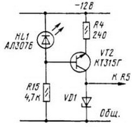
Transistor VT1 must be high-frequency or medium-frequency, with a permissible collector-emitter voltage of at least 50 V and a saturation voltage of not more than 0,5 V at a collector current of 100 mA. To accelerate the exit of the mid-frequency transistor from saturation when turned off, the capacitance of the capacitor C6 should be increased. The operational amplifier K140UD6 (DA1) can be replaced with KR140UD6 without changing the pattern of the printed circuit conductors of the board or with any other with field-effect transistors at the input. Transformer T1 is wound on an annular magnetic circuit of size K20 x 12 x 6 made of M1500NMZ ferrite. The primary winding contains 35 turns, and the secondary - 220 turns of PELSHO 0,2 wire. In order to reduce the interwinding capacitance, the wire of the secondary winding should be laid in one thick layer, gradually shifting along the magnetic circuit, while the first and last turns should be side by side. The primary winding is single-layer, it is wound over the secondary. The polarity of the winding leads does not matter. The inverter must be configured in this order. Disconnect the primary winding of the transformer from the transistor, and connect the upper (according to the diagram) output of the resistor R3 to the negative output of the power source through two resistors with a total resistance of 140 kOhm. When the engine of the tuning resistor R6 is rotated, the duty cycle of the pulses at the output of the DD1.4 element (control with an oscilloscope or a DC voltmeter connected between the output of this element and the common wire) should change abruptly from the minimum (about 0,1 or the pulses may disappear completely) to the maximum (0,65). Fix the trimming resistor engine in the position where this jump occurs. Then completely mount the converter, connect a voltmeter with an input resistance of at least 10 MΩ to its output and turn on the power. The output voltage can be controlled by the same voltmeter and by the voltage across the resistor R3 (5 V) or by a microammeter connected in series with this resistor (50 μA). Next, adjust the output voltage of the converter with resistor R6 and check the stability of its operation when the load and power supply voltage change. To reduce the interference emitted by the converter, it is placed in a brass case. If more noise suppression is required, a simple RC filter can be included in the secondary circuit of the converter, and a DM-0,1 inductor with an inductance of 400 μH and a feed-through capacitor can be included in the primary circuit. The described converter is designed to operate from a stabilized 12 V power source, in which a positive terminal is connected to a common wire. But without any changes in the installation, the negative terminal of the power source can be connected to the common wire. As an experiment, a variant of this converter powered by a bipolar source of ±12 V was tested. (according to the diagram) the output of the resistor R1 and the output of the primary winding of the transformer T30 are connected to the +12 V circuit. The values of the replaced elements: R12 - 14 kOhm, C1 - 12 pF, C13 - 1,1 pF, R6 - 1600 kOhm. Transistor VT7 - KT430G. The number of turns of the primary winding of the transformer T14 is doubled. If you use an unstabilized power supply, then the stabilization coefficient of the R4VD1 circuit may not be sufficient. In this case, the power supply circuit of the zener diode should be made according to the scheme shown in Fig. 134. The HL1 LED will serve as a power-on indicator. Author: Biryukov S.
Machine for thinning flowers in gardens
02.05.2024 Advanced Infrared Microscope
02.05.2024 Air trap for insects
01.05.2024
▪ Voice will betray depression ▪ Drawing color pictures with white light ▪ 4 Gb LPDDR8 DRAM Mobile Memory Chips ▪ Smartphone Vivo X3 thickness less than 6 mm ▪ Electrical stimulation of the brain helps to cope with a stroke
▪ site section Power Amplifiers. Article selection ▪ article Theater for yourself. Popular expression ▪ article What is a gentleman's agreement? Detailed answer ▪ article Common pear. Legends, cultivation, methods of application ▪ article ATS - a prefix to a computer. Encyclopedia of radio electronics and electrical engineering
Home page | Library | Articles | Website map | Site Reviews
www.diagram.com.ua |


 Leave your comment on this article: