|
|


 Arabic
 Bengali
 Chinese
 English
 French
 German
 Hebrew
 Hindi
Hindi Italian
 Japanese
 Korean
 Malay
Malay Polish
 Portuguese
 Spanish
 Turkish
 Ukrainian
 Vietnamese
|
ENCYCLOPEDIA OF RADIO ELECTRONICS AND ELECTRICAL ENGINEERING Car radio. Encyclopedia of radio electronics and electrical engineering
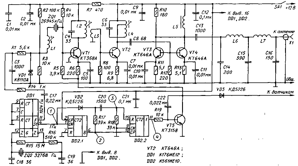
Encyclopedia of radio electronics and electrical engineering / Automobile. Security devices and alarms This device provides continuous monitoring of the state of the protected object over the radio. In case of any unauthorized impact on it or failure of the transmitter, the receiver will immediately notify the owner of this with an alarm signal. The radio channel of the described guard device consists of a transmitter installed in the car and a receiver located at the owner. In standby mode, the transmitter emits a frequency-modulated message every 16 s at a frequency of 26945 kHz (you can learn about the choice of radio channel parameters from publication [1]). The duration of the message is 1s, the modulation frequency is 1024 Hz. When security sensors are triggered, the transmitter switches to continuous modulated emission mode, to which the receiver will respond with an alarm signal. The same signal will sound if the receiver does not receive another message 16s after the beginning of the previous one. This algorithm of operation of the radio watchman ensures high reliability of protection, since any defect - damage to the antenna, discharge of the battery or failure of the transmitter - will immediately be marked with a warning signal. The output power of the transmitter is 2 W, the sensitivity of the receiver is better than 1 μV. With a small transmitter antenna mounted behind the windshield of a car and a receiver whip antenna about 50 cm long, the range of the radio channel exceeds 500 m. If, however, full-size antennas are used on the car and at the receiving place, the range can reach several kilometers. The watchman transmitter circuit is shown in fig. 1. A node is assembled on the DD1 and DD2 microcircuits, providing the necessary time rhythm of its operation. The master oscillator of the DD1 chip is stabilized by the "clock" quartz resonator ZQ2. The signal from the output F of the counter of the microcircuit DD1 [2] modulates the transmitter generator, and from the output S1 it goes to the input CN of the counter DD2.1 and the diode-capacitor switch VD2R17C20R18.
While the output 8 of the counter DD2.1 is low logic level, pulses with a frequency of 1 Hz pass through the switch and reset the counter DD2.2 (Fig. 2, diagrams 2 and 3). When a high logic level appears at the output 8 of the counter DD2.1, the diode VD2 closes and the pulses at the input R of the counter DD2.2 stop coming. At the moment of the appearance of a negative drop at the input of the SR counter DD2.2, it goes into a single state and a high logic level appears at its output 1.
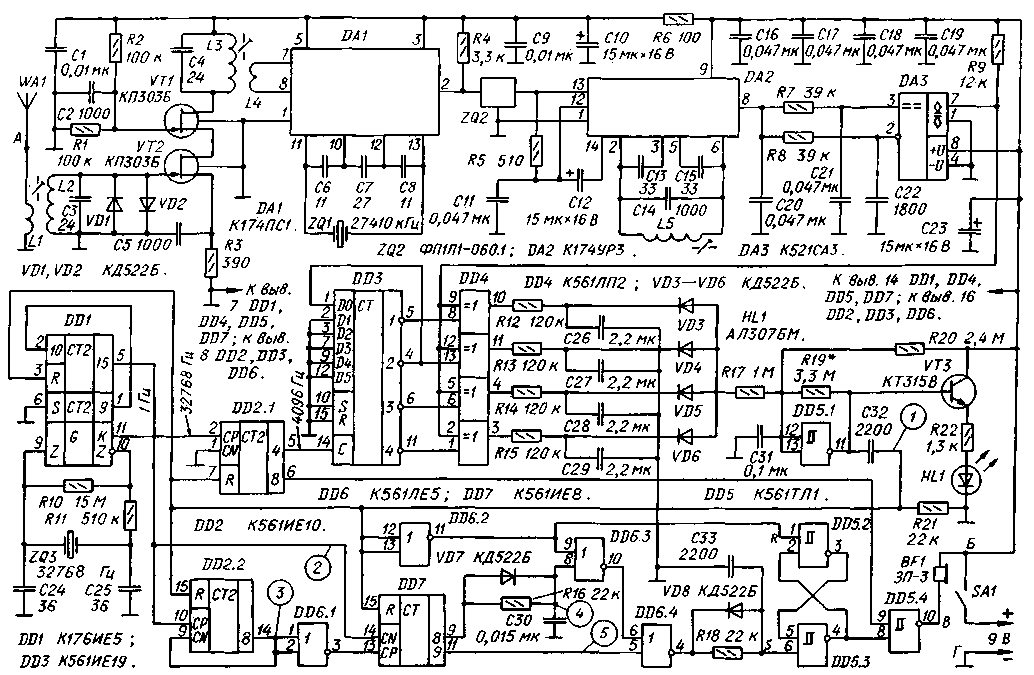
The next pulse from the output S1 of the counter DD1, passing through the opened diode VD1, resets the counter DD2.2. Thus, the counter DD2.2 generates at output 1 high-level pulses with a duration of 1 s with a repetition period of 16 s (Fig. 4). High-level pulses from the output of the counter DD2.2 open the switching transistor VT5, allowing the operation of the transmitter carrier generator. The transmitter is based on the device described in the brochure [3]. The generator is assembled on a transistor VT1 and stabilized by a quartz resonator ZQ1. A modulating signal with a frequency of 1024 Hz is applied to the VD1 varicap. Modulation - narrowband. The deviation within a small range is changed by the coil trimmer L1. Fluctuations in the operating frequency of the generator highlights the oscillatory circuit L2C4. Through the coupling coil L3, the signal is fed to the input of the buffer resonant amplifier on the transistor VT2, operating in mode C. The load of the transistor is the circuit L4C6. Through the capacitor C8, the amplified signal is connected to the input of the power amplifier, which is made on two parallel-connected transistors VT3 and VT4, also operating in C mode. wave impedance 13 Ohm. The transmitter switches to continuous radiation mode when security sensors are triggered, closing the cathode of the VD3 diode to the car body. If it is necessary to decouple the sensors from each other, several such diodes should be installed, the anode of which should be connected to the collector of the VT5 transistor. If any sensors generate a high-level signal at the time of operation, the output of each of them is connected to the base of the VT5 transistor through a series-connected resistor with a resistance of 20 ... 33 kOhm and any silicon low-power diode (cathode to the base). Receiver circuit the radio watch is shown in Fig. 3. The high-frequency part is assembled according to the traditional scheme. The signal received by the WA1 antenna is highlighted by the input circuit L2C3. Diodes VD1 and VD2 are used to protect the input of the RF amplifier with a large input signal amplitude. The RF amplifier is assembled according to a cascode circuit on field-effect transistors VT1 and VT2. The load of the amplifier is the circuit L3C4.
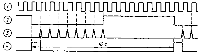
The mixer is made on the DA1 chip. It also performs the functions of a local oscillator, the frequency of which is stabilized by a ZQ1 quartz resonator. The resonator frequency can be higher or lower than the transmitter frequency by 465 kHz, i.e. either 26480 or 27410 kHz. From the mixer load - resistor R4 - the IF signal is fed to the piezoceramic IF filter ZQ2, which provides the necessary selectivity of the receiver. The DA2 chip performs signal amplification, clipping, and frequency detection. The resonant circuit C14L5 of the frequency detector is tuned to a frequency of 465 kHz. The demodulated signal with a frequency of 1024 Hz is fed to the inputs of the comparator DA3 through two integrating circuits that differ in the value of the time constant. The signal enters the direct input through the R7C21 circuit, which almost completely suppresses the useful signal, and the inverse signal comes through the R8C22 circuit with almost no attenuation. Such a node is a bandpass filter. At a frequency of 1024 Hz, it generates an output sequence of pulses that is close to a "meander" in shape, and input signals with a frequency that differs significantly from 1024 Hz practically do not pass to the output. From the output of the comparator DA3, the signal is fed to the input of the digital node. The rhythm of his work sets the generator on the DD1 chip, the frequency of which is stabilized by the same as in the transmitter, a quartz resonator at a frequency of 32768 Hz. The output pulses of the generator with a frequency of 32768 Hz from the output K are fed to the input of the CP counter DD2.1 of the frequency control channel, and with a frequency of 1 Hz from the output 15 of the counter of the microcircuit DD1 - to the input of the CP of the counter DD2.2 and the input CN of the counter DD7 of the time interval control channel . The DD2.1 counter generates pulses with a duty cycle of 2. The DD3 counter is a five-bit shift register, which, when output 2 is connected to the DO input, divides the pulse frequency by four [4]. At the same time, at outputs 1 - 4, it generates signals of the "meander" type with a phase shift of 0, 90, 180 and 270 °. These four signals are fed to the lower circuit inputs of the elements DD4.1 - DD4.4, and the output signal of the comparator DA3 is applied to the upper inputs, connected together. In the absence of a useful signal at the input of the receiver, a noise voltage acts at the output of the comparator. After mixing in the elements DD4.1 - DD4.4 with the output signals of the counter DD3, the noise is averaged by the integrating circuits R12C26, R13C27, R14C28, R15C29. As a result, the voltage across capacitors C26 - C29 is approximately half the supply voltage. At the input of the Schmitt trigger DD5.1, taking into account the drop on the diodes VD3 - VD6 and resistor R17, the voltage exceeds the upper switching threshold of the trigger, so its output will be a low logic level. When a voltage with a frequency of 1024 Hz appears at the output of the comparator, it is multiplied by the elements DD4.1 - DD4.4 with the output signals of the counter DD3. If the phases of the signals at the inputs of any of these elements coincide, its output will be low, with antiphase signals it will be high, and with close phases there will be high duty cycle pulses, and the average voltage of these pulses is close to zero. Therefore, approximately 0,5 s after the start of receiving the useful signal, one of the capacitors C26 - C29, corresponding to that element of the DD4 microcircuit, the phases of the input signals of which are closest, is discharged almost to zero. The voltage at the input of the Schmitt trigger DD5.1 becomes lower than the lower switching threshold, and a high level appears at its output. After about 0,5 s after the reception of the useful signal on the capacitors C26 - C29, a voltage close to half the supply voltage is again set, and the Schmitt trigger DD5.1 goes into its original state. Thus, high-level pulses are formed at its output, approximately corresponding in duration to the input and delayed relative to it by 0,5 s. The HL1 LED flashes for 1 s, indicating the presence of a useful signal in the WA1 antenna. Negative OS through the resistor R19 somewhat reduces the width of the "hysteresis" loop of the Schmitt trigger. The passband width of the peculiar filter mentioned above is about 2 Hz, and when the modulation frequency goes beyond 1023 ... 1025 Hz, the Schmitt trigger DD5.1 will not work. Let us consider how the digital processing unit acts after switching on when receiving signal packets with a frequency of 1024 Hz and a repetition period of 16 s. Circuit C32R21 differentiates the front of the pulse generated at the output of the element DD5.1. A short pulse of positive polarity - we will call it a control pulse (diagram 1 in Fig. 4) - enters the input R of the counters DD1, DD2.1, DD2.2, DD7, and also through the inverter DD6.2 to the input R of the trigger assembled on elements DD5.2 and DD5.3, transferring the trigger to the zero state. This short pulse also passes through the elements DD6.3 and DD6.4 at a low level at the outputs 8 and 9 of the counter DD7 and at the input S sets the trigger DD5.2, DD5.3 to a single state, in which the output of the element DD5.3 is high logical level.
The pulse at the input S of the trigger has a duration longer than at the input R due to the action of the R18VD8C33 circuit, therefore, after the pulse decays, the trigger remains in a single state, keeping the element DD5.4 open. Since the upper input of this element from the output 8 of the counter DD2.1 receives pulses of the "meander" type with a frequency of 2048 Hz, a continuous sound signal sounds. Pulses with a frequency of 1 Hz come from the output 15 of the counter DD1 to the input of the CP counter DD2.2 and CN - DD7 (Fig. 2). The first of them considers these pulses according to their decline, the second is blocked by a high level coming to the input of the SR from the output of the inverter DD6.1. After 8 s, a high level appears at the output 8 of the counter DD2.2 (diagram 3). It stops and self-blocks the counter DD2.2. The counter can exit this state only after the zeroing pulse arrives at its input R. The signal from the output of the counter DD2.2 after inversion element DD6.1 allows the counter DD7, counting second pulses on their front. After another 7,5 s, a high level appears at output 8 of this counter. Thus, after 15,5 s after the appearance of the control pulse, a high level will appear at the lower input of the DD6.3 element according to the circuit, which is held for 1 s (Fig. 4), if the input mode of the counter DD7 does not change during this time. When the next control pulse appears (16 s after the previous one), it switches the trigger DD5.2, DD5.3 to the zero state and the sound signal stops. The pulse does not pass through the elements DD6.3, DD6.4, because the lower input of the element DD6.3 is high. At the moment the control pulse arrives, all counters, including DD7, are reset to zero, however, at the lower input of the DD6.3 element, due to the action of the VD7R16C30 circuit, the high level change to low is delayed by about 200 μs. This guarantees the prohibition of the passage of a short control pulse (its duration is about 30 μs) to the input S of the trigger DD5.2, DD5.3. Therefore, when control pulses arrive, the trigger remains in the zero state and the signal does not sound. The described process is illustrated in fig. 4 solid pins. If the next control pulse does not arrive after 16 ± 0,5 s, the device will operate as shown in Fig. 4 dotted lines. The high level that appears after 16,5 s at the output 9 of the counter DD7 will set the trigger DD5.2, DD5.3 to a single state and a signal will sound. It will stop only when two pulses arrive at the receiver with an interval of 16 s between them. The signal will also sound if the pulse appears earlier than 15,5 s after the previous one, since there will be no prohibition from the output 8 of the counter DD7 on its passage through the element DD6.3. Thus, with the systematic arrival of signals with a modulation frequency of 1024 Hz and a period of 16 s, the system is in standby mode, the HL1 LED on its front panel flashes, indicating the health of the radio guard as a whole and the passage of radio signals. At any deviation from the specified rhythm, a signal starts to sound. The continuous glow of the HL1 LED means that some kind of security sensor is triggered, and the absence of glow means the transmitter stops working or the radio waves pass below the permissible level. Literature 1. Vinogradov Yu. Radio channel of the burglar alarm. Transmission block. - Radio, 1995, No. 1,0.37-40. Author: S. Biryukov, Moscow; Publication: N. Bolshakov, rf.atnn.ru
Artificial leather for touch emulation
15.04.2024 Petgugu Global cat litter
15.04.2024 The attractiveness of caring men
14.04.2024
▪ L'Oreal Colorsonic device for hair coloring ▪ Lavo home hydrogen batteries
▪ site section Preamplifiers. Article selection ▪ Article Private International Law. Lecture notes ▪ article Where was the flat-earth society until recently? Detailed answer ▪ article Cetraria Icelandic. Legends, cultivation, methods of application ▪ article The Incredible Knot. Focus Secret
Home page | Library | Articles | Website map | Site Reviews
www.diagram.com.ua |


 Leave your comment on this article: