|
|


 Arabic
 Bengali
 Chinese
 English
 French
 German
 Hebrew
 Hindi
Hindi Italian
 Japanese
 Korean
 Malay
Malay Polish
 Portuguese
 Spanish
 Turkish
 Ukrainian
 Vietnamese
|
Application of ADC KR572PV5. Encyclopedia of radio electronics and electrical engineering
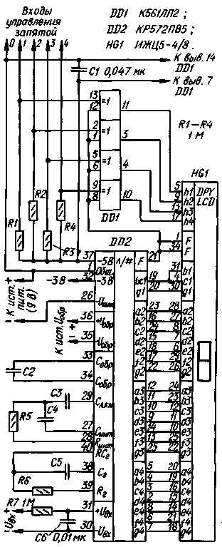
Encyclopedia of radio electronics and electrical engineering / Application of microcircuits The purpose of the ADC KR572PV5 is to convert the analog signal voltage into digital form for subsequent display of the signal level by a digital indicator. The device is designed to work together with a four-digit liquid crystal digital indicator. The KR572PV5 chip is manufactured using CMOS technology. The converter (fig. 1) consists of analog and digital parts. The analog one contains electronic switches S1-S11, a buffer op-amp DA1 operating in repeater mode, an integrator on the op-amp DA2, and a comparator DA3. The digital part includes generator G1, logic device DD1, pulse counter DD2, memory register with output decoder DD3.
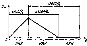
The converter uses the principle of double integration, according to which, at first, the discharged integrating capacitor Sint is charged for a certain time with a current proportional to the measured voltage, and then it is discharged with a certain current to zero. The time during which the capacitor discharges will be proportional to the measured voltage. This time is measured with a pulse counter; from its output, signals are sent to the indicator. The measured voltage Uin is supplied to the input of the converter (pins 30 and 31). and on the output 36 and 35 - exemplary Uarr. The measurement cycle (Fig. 2) consists of three stages - signal integration, i.e. charging the integrating capacitor (ICC), discharging the integrating capacitor (RIC) and automatic zero correction (ACC). Each stage corresponds to a certain switching of the elements of the converter, performed by switches S1-S11 on transistors of the MOS structure. On the diagram of Fig. 1 the inscriptions at the switches indicate the stage during which the "contacts" are closed. The duration of the stage, precisely set by the counter D02, is proportional to the period of the clock frequency ft.
During the stage of the ZIK, lasting 4000 periods of the clock frequency, the input signal through the switches S1, S2 and the buffer amplifier DA1 is fed to the input of the integrator DA2. This causes a charge accumulation on the Sint capacitor, proportional and corresponding in sign to the applied input voltage. The voltage at the output of the OA2 integrator changes at a constant rate proportional to the input signal. Suppose that by the beginning of the ZIK stage, the charge on the capacitors Sint and Sakn and the zero bias voltage of the op-amp DA1-DA3 are equal to zero (Sakn is the storage capacitor of the automatic zero correction unit). Since the input current of the DA2 integrator is small, there is no voltage change across the capacitor Sakn, and it actually does not affect the integration process. Capacitor Sobr remains charged from the previous cycle from the reference voltage source to Uobr. At the end of the ZIK stage, the comparator DA3 determines the sign of the input voltage by the sign of the voltage at the output of the integrator DA2. The sensitivity of the DA3 comparator is such that it correctly determines the polarity of the input signal, even if the signal is significantly less than one count. When the converter is operating at the RIC stage, the input signal to the integrator DA2 is not received. Switches S7, S8 or S6, S9 are connected to its input by the capacitor Sobr charged to the reference voltage, and in such a polarity (this is the reason for the choice of one or another pair of switches) at which the capacitor Sint is discharged. The discharge lasts until the capacitor Sint is completely discharged, i.e., the voltage at the output of the op-amp DA2 becomes zero. At this moment, the DA3 comparator connected in parallel with the Sint capacitor is triggered and completes the RIC stage. The charge of the capacitors Sobr and Sakn practically does not change. The discharge time of the capacitor Sint, expressed as the number of periods of clock pulses, is the result of the measurement recorded in the counter DD2. The state of the counter is rewritten to the DD3 register, and then, after decoding into a seven-element code, the signals are sent to the indicator. When the sign of voltage Uin is opposite to that indicated in fig. 1, element g1 of indicator HG1 indicates a minus sign. When overloaded, only the number 1 in the most significant digit and the minus sign (for negative voltage) remain on the display. Stage AKN begins with the termination of the counter DD2, when the logic device DD1 "closes the contacts" switches S3, S4 and S11. The resulting tracking system provides charging of the capacitors Sint and Sakn to a voltage that compensates for the "zero" offset of the operational amplifiers DA1-DA3. It remains unchanged during the next two stages of the ZIK and RIK. As a result, the error reduced to the input due to the "zero" shift and its temperature drift does not exceed 10 μV. The operation of all converter nodes is controlled by the built-in clock generator. The repetition rate of its pulses is determined by the external element Rg and Cr. To suppress mains interference with frequency values that are multiples of 50 Hz, the clock frequency should be chosen such that during integration, equal to 4000 periods of the clock generator Tt, an integer number Nc of mains voltage periods fit (the duration of the mains period is 20 ms). Thus, 4000Тт = 20 Nc ms, where Nc = 1, 2, 3, etc. Hence, 1m = 1/Tm = 200/Nc kHz, i.e. 200, 100, 67, 50, 40 kHz; smaller values are usually not used. The ratings of the frequency-setting circuits of the clock generator are calculated by the formula Cr = 0,45 / ft * Rg. To increase the frequency stability between terminals 39 and 40, a quartz resonator can be included (in this case, the elements Rg and Cr are not needed). When the converter is operating from an external generator, clock pulses are applied to the pin. 40; pin. 38 and 39 are left free. The input voltage limits of the device depend on the reference voltage Uobr and are determined by the ratio Uin.max=±1,999 Uobr. The current readings of the indicator should be expressed as a number equal to 1000 Uin / Uobr, but in practice they are lower by 0,1 ... 0,2%. The measurement period at a clock frequency of 50 kHz is 320 ms. In other words, the device makes 3 measurements per second. A typical circuit for switching on the converter, its connection with a liquid crystal indicator and four EXCLUSIVE OR elements necessary to control the decimal points of the indicator is shown in fig. 3. The converter is designed for unipolar power supply with a stable voltage ranging from 7 to 10 V. The positive wire of the power source is connected to the pin. 1, and negative - to the pin. 26. With a supply voltage of 9 V ± 1% and an ambient temperature of 25 + 5 ° C, the maximum current consumption does not exceed 1,8 mA, while the conversion error is not more than one least significant digit. The input resistance is determined only by leakage and significantly exceeds 100 MΩ.
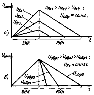
The converter is equipped with two built-in power supplies, one with a voltage of 2,9 ± 0,5 V, and the second with about 5 V. The plus of the first is connected to the pin. 1, and minus - with pin. 32 (this output is considered to be the common wire of the analog part of the converter). The second source has a plus on the same pin. 1, and minus - on pin 37. The first (three-volt) source is used to generate a reference voltage using a resistive divider. The change in the output voltage of this source when the supply voltage of the microcircuit fluctuates within 7,5 ... 10 V does not exceed 0,05%; the voltage temperature coefficient is positive and does not exceed 0,01% /°C. These parameters of the transducer provide a very high accuracy of the multimeter, built on its basis, when working in laboratory conditions (with fluctuations in air temperature within 15 ... 25 ° C) and quite acceptable for many measurements in a wider temperature range. At the same time, the output impedance of the source is quite large - at a load current of 1 mA, the voltage at its output drops by about 5%, at 3 mA - by 12%. Therefore, the indicated voltage stability is realized only at a constant load. If the load is connected to the pin. 26 and 32, the load current cannot exceed 10µA. This property of the source allows you to organize a bipolar power supply of the converter [1], in which the common wire of the two arms of the power supply will need to be connected to the pin. 32, the wire of the negative shoulder - to the pin. 26, positive - to the pin. one; supply voltage limits - 1x (2 ... 3,5) V. The second (five-volt) source is designed to power the control circuits of the liquid crystal display. The positive output of this source is vyv. 1, negative - pin. 37. The voltage stability of the source is worse than that of a three-volt one, by about 10 times. The load capacity is also low - at a load current of 1 mA, the output voltage decreases by 0,8 V, so it can be used almost exclusively to power the microcircuit that controls the LCD. At the output F, the converter generates a sequence of rectangular pulses of the "meander" type with a frequency 800 times less than the clock frequency (62,5 Hz at fт = 50 kHz). At the outputs connected to the elements of the indicator digits, the voltage has the same amplitude, shape and frequency, but it is in phase with the voltage at the output F for invisible elements and out of phase for visible ones. The low level of these pulses corresponds to -5 V (pin 37), and the high level corresponds to zero (pin 1). To tune the clock generator, it is convenient when the pulse frequency at the output F is equal to the mains frequency. The oscilloscope, on the screen of which they are observed, is synchronized from the mains and the clock generator is tuned to a frequency (near 40 kHz) at which the image becomes practically motionless. To control four decimal points, an additional four EXCLUSIVE OR gates (DD1 in Figure 3) are required. They repeat the "meander" phase for non-indicated commas and invert it for the one that should be visible. To indicate a particular comma, it is enough to connect the corresponding comma control input to the pin. 1 - a common point of power sources (the rest of the inputs are left free). When using the inclusion of the DD1 chip, this will mean that a high level is applied to the selected input. As already mentioned, the ADC on the KR572PV5 chip measures the ratio of the voltage values at the inputs Uin and Uobr. Therefore, there are two main options for its application. The traditional option - the voltage Uobr is unchanged, Vin varies within ±2Uobr (or from 0...2Uobr) [1-5]. The change in voltage across the capacitor Sint and at the output of the integrator DA2 (Fig. 1) for this case is shown in Fig. 4a. In the second variant, the voltage Uin remains constant, but Uobr changes. This variant was used in [6] and illustrated in Fig. 4,6. A mixed variant is also possible, when both Uin and Uar change with a change in the measured value (Fig. 3 in [7]).
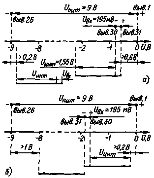
The voltage at the inputs and outputs of the OU, which are part of the converter, should not take them beyond the limits of the linear mode of operation. Typically, ±2 V limits are indicated, meaning the change in voltage relative to the analog common wire when using the built-in reference voltage source. Rice. 4 shows that the highest voltage at the output of the op-amp DA2 is determined by the maximum voltage at the input Uin of the converter. The sign of the voltage at the output of the integrator relative to the pin. 30 is opposite to the sign of the voltage on the pin. 31, and the Uint value can be calculated using the formula: Uint=4000Uin/(Sint*Rint*ft). (one). The voltage in this formula is expressed in volts, the capacitance is in microfarads, the resistance is in kiloohms, and the clock frequency is in kilohertz. Immediately, we note that in order to ensure the normal mode of discharging the capacitor Sint, the voltage on it must be less than the voltage between the pins. 1 and 32 with a margin of 0,2 ... 0,3 V. Therefore, it should not be more than 2 V with a unipolar power supply of the microcircuit and 3 .... 4 V (depending on the supply voltages) - with a bipolar one. To ensure maximum measurement accuracy, it is desirable that one of the extreme values of the voltage on the Sint capacitor, changing over a wide range, approaches the maximum possible. This determines the correct choice of the elements of the integrator Sint and Rint: Synt*Rint=4000Uin/(Uint*ft), (2), where the dimensions are the same as in (1). Recommended resistance values Rint=40...470 kOhm, and for the maximum voltage Uin it is necessary to choose Rint closer to the upper limit, for the minimum - to the lower one. The capacitance of the Sint capacitor is usually 0,1 ... 0,22 microfarads. To improve the measurement accuracy, it is recommended to connect one of the outputs of the sources of the measured and reference voltage to the analog common wire. However, it is of practical interest to differentially connect the converter inputs to their respective sources when none of the input terminals is connected to ground. In this case, the common-mode voltage (the common-mode voltage at the input is the arithmetic mean of two voltage values measured at one input terminal and at the other relative to any power wire) at the input can take any value from zero to Upit. The output signal of an ideal electronic device is independent of the common-mode voltage at its input. Such a device is said to completely suppress the common-mode interference voltage. In a real device, the common-mode voltage suppression is not complete, and this leads to all sorts of errors. The common-mode voltage suppression at the inputs of the KR572PV5 converter according to the passport is 100 dB, but its permissible limits are not indicated, at which the ADC still maintains the specified accuracy. Therefore, the limits of the common-mode voltage of the inputs Uin and Uobr were determined experimentally. The voltage Uobr is chosen equal to 100 mV, Uin - 195 mV, clock frequency - 50 kHz, Synth - 0,22 μF, Rint - 47 kOhm. For such a combination of parameters, the voltage Uint at the output of the integrator DA2 and on the capacitor Sint by the end of the ZIK stage, calculated by formula (1), is 1,55 V. The experiment consisted in the fact that with the help of two stabilized power supplies the common-mode voltage of one of the inputs was varied and the voltage measurement error was estimated according to the indications of the indicator board. The common-mode voltage of the other input and the values of Uin and Uobr remained fixed by means of resistive dividers. Then the other entrance was examined in the same way. During the experiment, it turned out that the input common-mode voltage Uobr can be changed in the full range of the supply voltage, provided Uobr<2 V and maintaining the specified polarity (Fig. 3). The voltage at each of the input terminals must not go beyond the interval. With the input Uin, the situation is more complicated. There are two cases to be considered here. If the input signal has the polarity corresponding to fig. 1 and 3, the voltage on the pin. 31 should be less (negative) than pin 1, not less than 0,6 V. This is determined by the range of linear operation of the op-amp DA1 as a follower. At the end of the ZIK stage, the voltage at the output of the DA2 integrator (pin 27) becomes Uint less than the pin. 30. The ratio of voltage levels at the terminals is illustrated by the diagram in fig. 5a - thick line in the lower right part.
As the input common-mode voltage approaches the lower limit of the Upit interval, the non-linearity of the operation of the op-amp DA2 begins to affect. For the op-amp on CMOS transistors, the range of linear operation of the op-amp is close to the full supply voltage, so the voltage at pin 30 should remain greater than at pin 26, to the Uint value plus a small margin (about 0,2 V) - the second thick line in the lower left part of Fig. 5, a. With the opposite polarity of the input signal, the voltage at the output of the integrator is higher by Uint than at the pin. 30 (Fig. 5,6), therefore it is it that determines the allowable voltage on the pin. 30 near the upper limit of the voltage on the pin. 1. It has been experimentally determined that the margin should also not be less than 0,2 V, therefore, for Uint \u1,55d 1 V, the difference Uvy.30 - Uvy.1,75 must exceed XNUMX V. With the approach of the common-mode input voltage Uin to the voltage at the pin. 26 again the main role begins to play the allowable range of linear operation of the OS DA1. The minimum allowable difference Uvyv.31 - Uvyv.26 - about 1 V (Fig. 5,6). Thus, the thick lines show the extreme positions of the sum Uint + Uin on the voltage coordinate axis both for one and the other polarity Uin. From the results obtained, it follows that in order to measure the signal voltage, the common-mode component of which is as close as possible to the voltage at the pin. 1, the signal source should be connected in the polarity shown in fig. 1 and 3. If the common-mode component is close to the voltage at the pin. 26, the polarity of the connection must be reversed. With a variable polarity of the measured voltage, in order to obtain the widest possible limits of the permissible common-mode voltage, it is possible to reduce the voltage Uint at the output of the integrator, for example, to 0,5 V by increasing the capacitance of the capacitor Sint or the resistance of the resistor Rint in accordance with formula (2). When the voltage at the input Uin during the operation of the ADC does not change polarity, you can abandon the capacitor Collect. but the exemplary voltage will need to be applied to the pin. 32 and one of the pins for connecting this capacitor. The exemplary voltage can be applied as a plus to the pin. 33, and minus - to the pin. 32, but then the polarity of the input voltage must be reversed. The indicator will "highlight" the minus sign (if, of course, this element of the indicator is connected). In cases where it is undesirable to change the polarity of the connection of the voltage Uin, it is possible to apply the voltage Uobr in another way. - plus to vyv. 32, minus - to the pin. 34. There will be no minus sign on the display, but the built-in three-volt source will be unsuitable for the formation of an exemplary voltage. To reduce the influence of parasitic mounting capacitance on measurement accuracy, especially at high values of common-mode voltage, it is recommended to provide a ring conductor on the printed circuit board, covering the installation site of Sint, Uint and Sakn elements. This conductor is connected to the pin. 27 chips. When using a double-sided printed circuit board, on the reverse side opposite the ring conductor, you should leave a foil shielding pad connected to the same pin. 27. Chain R7C6 in fig. 3 serves to protect the output + Uin from static electricity in those cases when it can be connected to any elements outside the measuring device case, and the output -Uin - to a common wire. If it is possible to connect other ADC inputs to external circuits, they are also protected by similar circuits (as is done, for example, in the multimeter [3] for the Uin input). The resistance of the protective resistors of the Uoep input must be reduced to 51 kΩ, otherwise the settling time of the instrument will be too long. About the capacitance of capacitors Cobr and Saqn. The following values are recommended in various literature: for a maximum input voltage of 200 mV Collect = 1 μF, Saqn = 0,47 μF; the same for Uin \u2d 0,1V-0,047 and 35 microfarads. If during operation the voltage Uobr (supplied to pins 36 and 2,6,7) is unchanged, then to increase the accuracy of the ADC, the capacitance Collect can be increased several times relative to the indicated values, and if it can * change (as, for example, in [XNUMX ,XNUMX]), it is undesirable to significantly increase the capacitance, since this will increase the time for setting the readings. The capacitance of the capacitor Sakn significantly affects the settling time of readings after overloading the input of the converter. Therefore, in all the mentioned devices (except for thermometers [4, 5], where overload is practically impossible), it is desirable to adhere to the capacitance values recommended above. The Sint integrator capacitor must be with a dielectric with low absorption, for example, K71-5, K72-9, K73-16, K73-17. To reduce the settling time of readings in cases where the voltage on the Sovr and Sakn capacitors can change, it is desirable to use the same capacitors for them. If the voltage on them does not change, it is permissible to use ceramic capacitors, for example KM-6. Since the principle of double integration is characterized by insensitivity to changes in the clock frequency or integration rate (within reasonable limits), there are no special requirements for the stability of the resistor Rint and the frequency-setting elements of the ADC generator. The resistors of the divider that determines the voltage Uobr must, of course, be stable. Now I would like to briefly comment and clarify the choice of some elements published in the journal of digital measuring instruments on the ADC KR572PV5, published in the journal "Radio". Multimeter [2]. The capacitance of the integrator capacitor C3 (Fig. 1) or the resistance of the integrator resistor R35 can be doubled, which will eliminate the need to select the resistor R35. This will also allow you to set the clock frequency (50 kHz) once during setup, while monitoring the frequency of the signal at the output F (62,5 Hz). The storage capacitor C2 (Collect) can be used ceramic KM-6. All of the above applies to the multimeter [3]. Capacitance meter [7]. It is better to reduce the capacitance of the integrator capacitor C11 (Fig. 1) to 0,1 microfarads, and C 14 (Sacn) - increase to 0,22 microfarads. To reduce the settling time of readings, it is advisable to choose capacitors C 10 (Col) and C14 with a good dielectric. Since the sign of the voltage at the input Uin ADC does not change, the capacitor C10 can be excluded. To do this, the upper terminal of the capacitor C9 according to the scheme should be switched to the pin. 33 DD5 microcircuits (it is possible without disconnecting from pin 36) and change the conductors to pin. 30 and 31. RCL meter [1]. It is desirable to increase the capacitance of the storage capacitor C19 (Fig. 2) to 1 microfarad, but it can be excluded by connecting the lower output of the resistor R21 according to the circuit and the pin. 35 microcircuit DD10 with its pin. 32, trimmer resistor engine - with pin. 33 and, changing the conductors among themselves, to the pin. 30 and 31; resistor R22 is also excluded. And in conclusion, a few words about the possibility of combining structures. The temptation of such a combination is that it is not necessary to purchase an expensive microcircuit and indicator for each device, to assemble a rather laborious assembly. We note right away that all meters, except for [1, Z], are insensitive to the clock frequency, if, of course, it is selected from the recommended series with the corresponding recalculation of the element ratings. To switch from a frequency of 50 to 40 kHz, it is enough to increase the resistance of the integrator resistor Screw by 20%, for a frequency of 100 kHz, reduce the capacitance of the capacitors Sint, Sobr, Sakn by half. While maintaining the ratings of the elements of the RCL meter [1] and the frequency of its clock generator of 40 kHz, any other device can be combined with it, except for the capacitance meter [7]. Conversely, with a meter [7] with the above clarification for Sint and Sakn and a clock frequency of 100 kHz, it is permissible to combine any other design, except for [1]. In the absence of ADC KR572PV5 or liquid crystal indicator IZhTs5-4/8, the meters described here can be assembled on KR572PV2 and LED digital indicators with a common anode, as, for example, it was done in [8,9]. All recommendations of the article you are reading now are also applicable to devices based on the KR572PV2 ADC. Note that the multimeter [8, 9] uses a symmetrical power supply of the converter, so the choice of the value Xin = 0,1 μF is quite justified. In devices based on the ADC KR572PV2, a separate source of 4 ... 5 V for a current of about 100 mA should be used to power the LED indicators. Its negative terminal is connected to the pin. 21 microcircuits (digital common wire), which does not have to be connected to a common analog wire. Note that when using LED indicators, their total current flowing through the internal circuits of the converter depends on the displayed number. Therefore, during the measurement process, the temperature of the microcircuit crystal changes, which significantly changes the voltage of the three-volt source and reduces the accuracy of the readings. That is why a separate exemplary source is used in the multimeter [8, 9]. The option of connecting vacuum luminescent indicators to the ADC KR572PV2A is described in [4]. Literature 1. Biryukov S. Digital meter RCL-Radio, 1996, No. 3, p.38-41; No. 7, p.62; 1997, No. 7, p. 32. Author: S. Biryukov, Moscow; Publication: N. Bolshakov, rf.atnn.ru
Machine for thinning flowers in gardens
02.05.2024 Advanced Infrared Microscope
02.05.2024 Air trap for insects
01.05.2024
▪ Passenger aircraft without windows ▪ Desalination of sea water based on nanofiber membrane ▪ Ultra-fast Samsung PM1725 and PM1633 SSDs ▪ Magnetic material properties: from insulator to metal
▪ section of the site Calls and audio simulators. Article selection ▪ article I'm not a coward, but I'm afraid! Popular expression ▪ article Where is left-hand traffic used? Detailed answer ▪ Article Four-loop knot. Travel Tips ▪ article Sound relay. Encyclopedia of radio electronics and electrical engineering
Home page | Library | Articles | Website map | Site Reviews
www.diagram.com.ua |


 Leave your comment on this article: