|
|


 Arabic
 Bengali
 Chinese
 English
 French
 German
 Hebrew
 Hindi
Hindi Italian
 Japanese
 Korean
 Malay
Malay Polish
 Portuguese
 Spanish
 Turkish
 Ukrainian
 Vietnamese
|
Network in the dimensions of the crown. Encyclopedia of radio electronics and electrical engineering
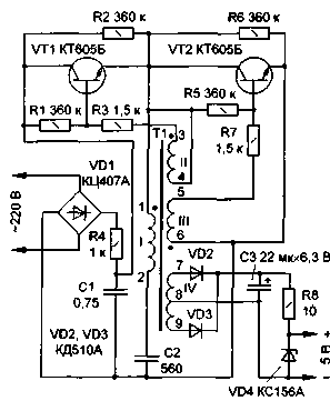
Encyclopedia of radio electronics and electrical engineering / Power Supplies The small dimensions of the device are achieved due to the fact that small-sized parts are used in it. Transistors dissipate little heat: when current flows through them, they are fully open. The source is not critical to shorting the output. The power supply circuit is shown in fig. 1. Operating points of transistors VT1, VT2 resistors R1, R3, R5, R7 brought to the limit of the cut-off mode. The transistors are still closed, but the conductivity of the collector-emitter section is increased, and even a slight increase in the voltage at the base will lead to the opening of the transistors: i.e., the voltages from the secondary windings of the transformer T1, necessary for control, are reduced. To create conditions for self-generation, it would be necessary to increase the conductivity of the transistors even more, but this cannot be done by further increasing the voltage at the base, because the conductivity will be different for different transistors and will change as the temperature changes. Therefore, resistors R2, R6 are used, connected in parallel with transistors.
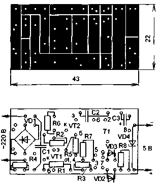
When the power supply is turned on, the smoothing capacitor C1 is charged through the resistor R4, which protects the diode bridge VD1 from overload. Applying an input voltage causes a voltage to appear at the output of the trigger divider formed by resistors R2 and R6. This voltage is applied to the oscillatory circuit from the primary winding of transformer T1 and capacitor C2. In the secondary winding II, an EMF pulse is induced. The power of this pulse is sufficient to introduce the transistor VT1 into saturation, since at the initial moment the current does not pass through it due to the self-induction of the transformer T1. Then the current begins to flow from the secondary winding II, holding the transistor VT1 in the open state. Transistor VT2 during this half-cycle of the oscillatory process is completely closed. It is held in this state by the EMF induced in the secondary winding III. After charging the capacitor C2, the current passing through the transistor VT1 stops and it closes. In the second half-cycle of the oscillatory process in the circuit (T1, C2), the current at the initial moment, when the transistors are still closed, passes through the second arm of the triggering divider (parallel connected resistor R6 and the collector-emitter section of transistor VT2). Similarly, the transistor VT2 opens and then is held in a fully open state. After discharging the capacitor C2, the current through the transistor VT2 stops and it closes. Thus, the current passes through the transistors only when they are fully open and have a minimum resistance of the collector-emitter section, so the heat loss power is small. High-frequency oscillations rectify the diodes VD2, VD3, the ripple is smoothed out by the capacitor C3. The output voltage is maintained by a constant zener diode VD4. A load with a current consumption of up to 40 mA can be connected to the output of the power supply. With a higher current, low-frequency ripples increase and the output voltage decreases. The insignificant heating of the transistors, which does not depend on the outflow of the load, is explained by the fact that in this device it is possible to pass through current through the transistors, when the first transistor has not yet had time to completely close, and the second one has already begun to open. The power supply can be used up to closing the output, the current of which is 200 mA. The transformer is made on a ring ferrite magnetic circuit K10X6X5 1000NN. Windings I, II, III, IV contain, respectively, 400, 30, 30, 20 + 20 turns of PELSHO 0,07 wire. To increase reliability, it is necessary to isolate the windings from one another with transformer paper. Any magnetic circuit with close initial permeability and dimensions can be used. Capacitor C2 - KM-4 or any other specified capacity for a rated voltage of at least 250 V. In the absence of small-sized high-voltage capacitors in place C1, it is permissible to use five capacitors KM-5 of the H90 group connected in parallel with a capacity of 0,15 μF. Although the manuals indicate that their nominal voltage is 50 V, in practice most of them withstand a constant input voltage. Their breakdown will not cause any serious consequences, since the resistor R4 will act as a fuse. Capacitor C3 - K53-16 or any small-sized one with a capacity and a rated voltage not lower than those indicated in the diagram. All resistors are C2-23, MLT or other small ones. Heatsinks for transistors are not required. The operating conversion frequency is about 100 kHz at a current consumed by the load of 50 mA. The higher the operating frequency of switching transistors, the lower the inductance the oscillating circuit can have, and, consequently, the smaller the dimensions of the transformer and the entire power source. A properly assembled power supply should immediately start working. However, if the transistors get very hot (which means they do not open completely), resistors R3, R7 are selected and R1, R5 are proportional to them. Output voltage may vary. To do this, change the number of turns of the winding IV and replace VD4 with another zener diode. If you need to have several values of the output voltage, use a series of zener diodes connected in series. The source can power devices made on digital microcircuits and other equipment that is insensitive to interference. It is not suitable for powering radio receivers due to high noise. The interference radiated into the air and induced into the network is weak, since the power of the source is low. The screen of the device is a case from the Krona battery. See [1-3] for more details about the different power supply options. On fig. 2 shows a drawing of a printed circuit board. The board is made of one-sided foil fiberglass or getinax.
It can be made without etching by removing the foil along the lines with a cutter. Transistors should be installed one slightly higher than the other so that their cases do not touch. The numbers indicate the holes corresponding to the numbers of the terminals of the transformer T1 (see Fig. 1). Pins 1 and 4 are soldered in one hole. Capacitor C1 is located above the diode bridge. Network wires are fixed with a bracket soldered into the board. Transformer T1 is put on a wire pin soldered to the board. An insulating tube must be put on this pin. The output block is soldered with short thick wires to the terminals of the zener diode. Resistors and diodes are mounted vertically. The assembled block is isolated with paper or film from the metal case of the Krona battery, in which it is placed. When installing and setting up the device, the well-known precautions for working with a 220 V network should be observed. Literature
Author: V. Solonin, Konotop, Sumy region, Ukraine; Publication: N. Bolshakov, rf.atnn.ru
Machine for thinning flowers in gardens
02.05.2024 Advanced Infrared Microscope
02.05.2024 Air trap for insects
01.05.2024
▪ Tommy Hilfiger Jacket with Integrated Solar Panels ▪ Optimists are not afraid of a heart attack ▪ Nvidia GeForce GTX 690 is the fastest graphics card
▪ section of the site Mobile communications. Article selection ▪ article All this would be funny if it were not so sad. Popular expression ▪ article What is the Red Planet? Detailed answer ▪ article Selector of reference and informational material. Job description ▪ article Semiconductor voltage limiters. Encyclopedia of radio electronics and electrical engineering
Home page | Library | Articles | Website map | Site Reviews
www.diagram.com.ua |

 Leave your comment on this article: