|
|


 Arabic
 Bengali
 Chinese
 English
 French
 German
 Hebrew
 Hindi
Hindi Italian
 Japanese
 Korean
 Malay
Malay Polish
 Portuguese
 Spanish
 Turkish
 Ukrainian
 Vietnamese
|
ENCYCLOPEDIA OF RADIO ELECTRONICS AND ELECTRICAL ENGINEERING VHF transverter. Encyclopedia of radio electronics and electrical engineering
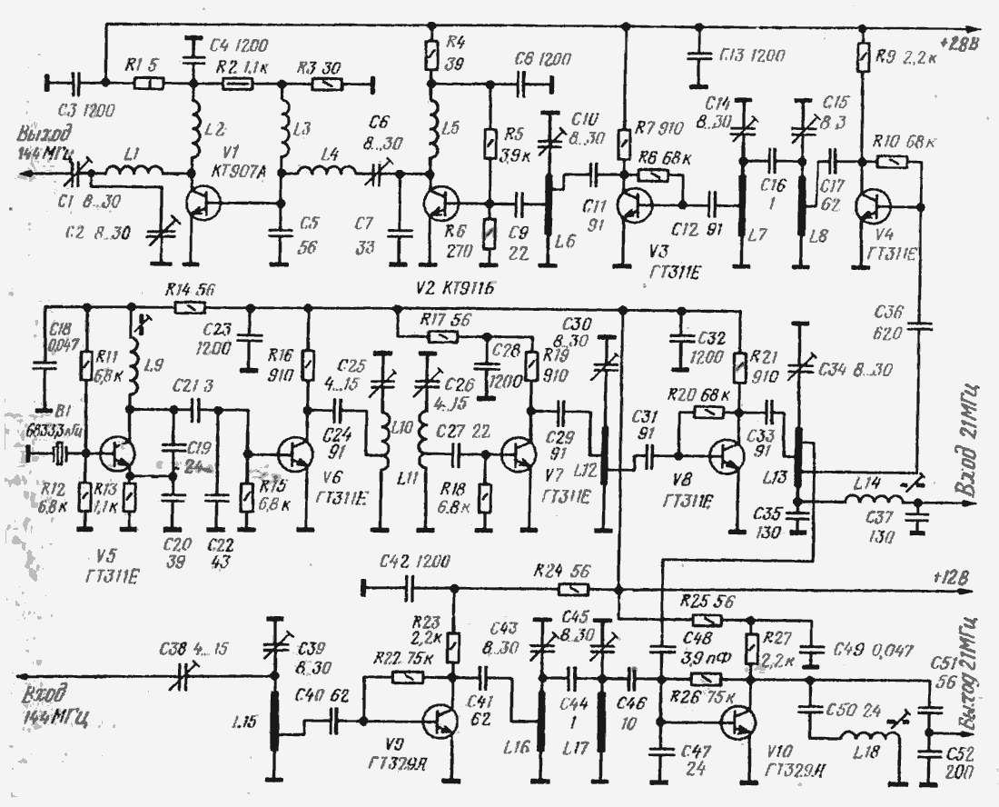
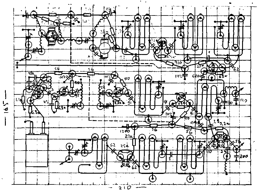
Encyclopedia of radio electronics and electrical engineering / Civil radio communications This 144...144,5 MHz transverter is designed to work in conjunction with a shortwave transceiver with a range of 21...21.5 or 28...28.5 MHz. The output power of the transverter in transmit mode is 5 W (at a power level coming from the transceiver of about 1 mW). The noise figure in the receive mode is 2...2,6 kTo (with the noise figure of the receiving part of the KB transceiver not more than 10...15 kTo). The transverter has a linear transmission path, i.e. it provides a linear relationship between the amplitude of the signal supplied from the KB of the transceiver and the amplitude of the output signal (in the range of 144 MHz). The schematic diagram of the transverter is shown in fig. 1. It can be divided into three main parts: receiving (transistors V9, V10) and transmitting (V1-V4) paths and a local oscillator common to them (V5-V8). The quartz self-oscillator of the local oscillator is made on the V5 transistor according to the capacitive "three-point" scheme. The choice of the desired mechanical harmonic of the quartz resonator is provided by the appropriate tuning of the L9C19C20 circuit. In this case, the quartz resonator 6833,3 kHz (6444.4 kHz) (hereinafter, in brackets are the frequencies for the transverter, which has an intermediate frequency of 28 ... 28,5 MHz.) Excited at the third mechanical harmonic, i.e. at a frequency of 20,5 .19,333 MHz (XNUMX MHz). From the oscillator, the signal first goes to the frequency tripler (transistor V6), the load of which is the band-pass filter L10C25L11C26. tuned to a frequency of 61,5 MHz (58 MHz), then to a doubler (transistor V7) and then to an amplifier (transistor V8). Filtering the output signal of the local oscillator with a frequency of 123 MHz (116 MHz) is provided by the L12C30 and L13CS4 circuits. The receiving path contains an RF amplifier and a mixer. The amplifier is assembled on a V9 transistor connected according to a common emitter circuit. The selected scheme for stabilizing the operation mode of the transistor in direct current (with the help of resistor R22) allows you to directly, without blocking capacitance, ground the emitter of the transistor. This provides a high stable stage gain. To improve the efficiency of the input circuit, the L15C39 circuit is strongly coupled to the base circuit of the transistor V9. The connection of the amplifier with the antenna is capacitive. Capacitors C38, C40 and coil L15 form a high-pass filter that prevents interference from powerful shortwave radio stations from penetrating the output of the converter. RF amplifier load - bandpass filter L16C4SL17C45. The signals of the local oscillator and the high-frequency amplifier are summed in the mixer (transistor V10). The matching of the mixer with the receiver input is provided by the L18C50C51C52 circuit. The transmission path begins with a mixer made on the transistor V4. The local oscillator voltage is supplied to the base of the transistor V4 from the L13C34 circuit. The CW, AM or SSB signal formed in the transceiver is fed to the mixer through the L14C35C37 circuit. The mixer load is an L8C15L7C14 band pass filter tuned to 144 MHz.
The converted signal is amplified by a three-stage linear amplifier. The first stage on the transistor V3 operates in class A mode. For better filtering of spurious radiation, the transistor is loosely connected to the input L7C14 and output L6C10 circuits. The main gain (about 20 dB) is provided by the second stage, on the transistor V2. It also operates in class A mode. The final stage operates in class AB mode. The required bias to the base of the transistor V1 comes from the divider R2R3. To prevent self-excitation (the so-called throttling self-oscillations), the upper output of the choke L3 according to the circuit is not blocked by a capacitor. The matching of the terminal amplifier with the antenna provides the L1C1C2 circuit. As the practice of working with a transverter made according to this scheme has shown, a simple modification of the output circuit (capacitor C2 is connected not to coil L1, but to the output of the device, modification of the circuit board is obvious - capacitor C2 in this case must be installed to the left (see tab) of capacitor C1 ) makes it possible to improve the filtering of spurious radiation. The adjustment of the structure will be described in relation to this, more advanced version. Since the transmitter does not have an output transistor protection device, it follows. avoid the operation of the output stage on a highly mismatched load. Construction and details There are no screening barriers in the transverter design, but this does not lead to self-excitation of the device: mounting the elements at a low height above the metal surface ensures a low level of parasitic interstage couplings. The transverter circuits operating at frequencies above 100 MHz have a somewhat unusual appearance. These are quarter-wave resonators shortened by capacitance, curved to reduce dimensions. The quality factor of an unloaded resonator is approximately 250. Almost the same quality factor can be obtained with a conventional silver-plated wire circuit. However, it has a larger stray field, and in this case, additional measures for shielding the transverter cascades cannot be dispensed with. Quarter-wave resonators are made of silver-plated wire with a diameter of 0,8 ... 1 mm. The line height above the board is about 2,5 mm. As the height decreases, the stray field decreases, but the quality factor also decreases. To give rigidity, the line rests on five platforms, for which, in the places of bending, the line is additionally bent in the horizontal plane at an angle of about 45°. Only on the site closest to the "earth" output of the resonator, the line is supported by a small piece of wire. It should be immediately noted that the dimensions of the line and its configuration are not very critical, since the trimmer capacitor provides tuning of the resonator in a very wide frequency range. The board has a groove between the first stages of the local oscillator and the output stages of the transmitting path. It plays the role of a thermal insulator that prevents the crystal oscillator parts from being heated by heat propagating from the output stages along the foil. All low-power transistors are inserted from the back of the board into holes drilled in it. Transistors are based on the rim on their case. If the thickness of the board exceeds 1 ... 1.5 mm, then the holes intended for transistors V9, V10 must be countersunk on the reverse side with a drill of a larger diameter so that the bottom of the transistor is flush with the foil. For the transistors of the last two stages of the transmission path, equipped with radiators, it is necessary to make holes in the board with a diameter equal to the outer diameter of the transistors. It is better if the holes are hexagonal, as this will prevent the transistor from rotating when the heatsink is attached. In the output stage, a KT907A transistor is used, in which the emitter terminal is connected to the case. To reduce the inductance of the emitter terminal, a copper foil spacer must be inserted between the transistor and the heatsink. The ends of the gasket are soldered to the board. The length of the terminals of the capacitor C5, connected between the base and the emitter of the output transistor, must be minimal. Mounting is carried out on reference points, which are formed by annular grooves cut in the foil. Groove width - 0,5 ... 0,8 mm. The diameter of the support circle is about 5 mm.
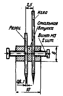
For the manufacture of such grooves, you can use the simplest device, the device of which is shown in Fig. 2. The device consists of a needle, a miniature cutter and a fastener. The needle and the cutter are made from used dental burs. To sharpen them, it is convenient to use an abrasive stone or a diamond file. The fastener is made of a steel sleeve with a diameter of 6 mm. The burs are inserted into two holes drilled in the sleeve and secured with two MXNUMX screws. For reliable fastening of burs, it is desirable to shine a chamfer on their side surfaces. The shank of the needle must be longer than the shank of the cutter so that it can be fixed in the drill. However, it will not be difficult to make annular grooves by hand. To do this, it is convenient to clamp the fixture in a hand jewelry vise. Do not apply excessive force and try to cut the groove in one go, as this will cause the foil to tear. Solder the details "in the overlay". The dotted line on the tab shows the conductors located on the reverse side of the board. They are passed through holes drilled near the respective pads. When selecting parts for a transverter, it is useful to consider that the values of most capacitors are not critical. This primarily applies to blocking capacitors in power circuits, the capacitance of which can be changed from 500 to several thousand picofarads. The capacitances of separating capacitors that connect transistors with resonant circuits are also not critical. Their values can be changed from -50 to +100%. Inductors L2, L3 and L5 are frameless, made of a piece of wire PEV-2 0,3 about 150 mm long. The wire is wound on a mandrel with a diameter of 2,6 mm. Coils L1, L10, L11 are frameless, wound on a mandrel with a diameter of 9 mm with a silver-plated wire with a diameter of 0,8 mm. Coil L1 contains 3 turns (winding length 7 mm), L0 and L11 each 8 turns (winding length 14 mm). In the L10 coil, the tap is made from the 1,25th Turn, in the L11 coil, from the 3,75th turn, counting from the bottom according to the output circuit. Coils L9, L14, L18 are wound on frames with a diameter of 5 mm with PEV-2 0.15 wire. The number of turns is 18. Carbonyl iron cores with M4 thread are used for adjustment. The transverter uses capacitors KM and KT, resistors M + and MLT. Setting up a transverter should start with a quartz oscillator. First of all, it is necessary to temporarily connect the base of the transistor V1000 with the case through a capacitor with a capacity of 5000-5 pF. In this case, the quartz oscillator will turn into a regular LC oscillator. The generation frequency in this case will be determined by the L9C19C20 circuit. By rotating the coil trimmer. L9 it is necessary to set it close to the triple frequency of the quartz resonator. After that, the capacitor from the base of the transistor V5 is disconnected and the position of the trimmer is found in which it has the least effect on the generation frequency. Then proceed to setting the frequency multipliers. When setting them up, as well as all other stages of the transverter, it is necessary to control the operating modes of transistors for direct current. It is most convenient to measure the voltage at the collector, since with a known resistance of the resistor in the collector circuit, it is easy to determine the current flowing through the transistor. Measurements must be made through a resistor with a resistance of at least 10 k0m. It must be fixed on the tip of the probe like this. so that the conductor connected to the elements of the transverter has a minimum length. Obviously, in the presence of an additional resistor, the voltmeter readings will be underestimated, but the resulting error is easy to take into account. Establishing a tripler begins with adjusting the excitation mode. By selecting capacitor C22, it is necessary to ensure that the constant voltage on the collector of transistor V6 is 5 ... 6 V. This corresponds to a collector current of the transistor of about 6 mA. After that, they start setting up the dual-circuit filter L10C25L11C26. The setting is made to the maximum collector current of the transistor V7. The required degree of excitation of the transistor V7 can be adjusted by changing the turn-on ratio of the filter circuits. When selecting taps on coils, care must be taken that both circuits are loaded approximately equally. If one of the circuits has a more "dumb" setting, then the tap on the coil should be moved closer to the lower output according to the circuit. With the filter set correctly, the DC voltage at the collector of the transistor V7 should be within 5 ... 6 V. If the dimensions of the coils L10 and L11 are maintained fairly accurately, and the trimmer capacitors are approximately in the middle position. Then the danger of setting the filter to the wrong harmonic is small. However, especially if the dimensions of the coils or the frequency of the crystal oscillator are changed, it is useful in one way or another to check the correct setting. You can, for example, use a receiver operating in the desired frequency range. A piece of wire must be connected to the input of the receiver, the other end of which should be brought to the L10C25 circuit. When rotating the tuning capacitor C25, the maximum volume of the signal should coincide with the maximum collector current of the transistor V7. The possibilities of this test method are limited by the fact that most communication receivers have an operating frequency range of no more than 25 MHz. You can expand the range of received frequencies using the simplest set-top box, the diagram of which is shown in Fig. 3.
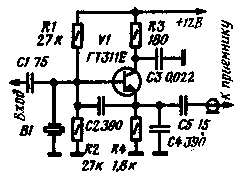
The prefix is a quartz self-oscillator, made on the transistor VI. It can use any quartz resonator with a natural frequency within 8 ... 15 MHz. At the same time, the transistor performs the functions of a mixer operating on the frequency harmonics of a quartz self-oscillator. The oscillator is connected with a piece of cable to the input of a shortwave receiver. When establishing a heterodyne path, the prefix must be connected to the circuit of a tunable multiplier using a short piece of mounting wire. To do this, bring the insulated end of the mounting wire to the "hot" output of the loop coil. Since there are no selective circuits in the set-top box, reception occurs simultaneously on many harmonics of the oscillator. It helps to understand the emerging mass of signals that the frequencies of the local oscillator crystal oscillator and the set-top box crystal oscillator are known in advance. As an example, consider the process of tuning the L10C25 circuit to a frequency of 61,5 MHz. Let the set-top box use a quartz resonator at a frequency of 9620 kHz, and checking the transverter's crystal oscillator showed that its frequency is 20504 kHz. In this case, the signal at the tripler output will have a frequency of 61 kHz. Such a signal can be listened to using the fourth or fifth harmonic of the local oscillator of the set-top box. In the first case, the signal should be sought at a frequency of 512 kHz (23032-61512 * 9620). In the second option, which is suitable for receivers with a narrower operating range, the signal must be sought at a frequency of 13412 kHz (61612- -9620 * 6). In this way, you can control the correct settings of the multipliers up to frequencies of 400 ... 500 MHz. In principle, the frequency range can be further expanded if a higher-frequency transistor is used and the capacitance of capacitors C2, C4 is reduced. The correct setting of the multipliers can also be checked with a resonant wavemeter. After the necessary excitation has been applied to the base of the transistor V7, they begin to tune the L12C30 circuit to a frequency of 123 MHz (116 MHz). The stage following the doubler is an amplifier based on a V8 transistor operating in class "A". The collector current of transistor V8 is weakly dependent on the amount of excitation, so it cannot be used to indicate the setting of the L12C30 doubler circuit. The adjustment must be made using a receiver or, in the simplest case, using a high-frequency probe connected to an avometer. The probe circuit is shown in fig. 4. The autometer should be switched to the most sensitive DC scale. The extent to which the probe is connected to the configurable node can be adjusted by moving the probe connection point to the loop.
After the L12C30 circuit is tuned to the desired frequency, they proceed to the establishment of the final amplifier of the heterodyne path. First of all, in the absence of an excitation signal, by selecting the resistor R20, it is necessary to set the collector current of the transistor V8 in the range of 7 ... 8 mA. After that, an exciting voltage must be applied to the V8 transistor and, using a high-frequency probe, adjust the L13C34 circuit. The establishment of the receiving path begins with the setting of the modes of transistors V9 and V10 for direct current. By selecting resistors R22 and R26, the collector currents of these transistors should be set within 2 ... 2,5 mA. After that, the mixer is connected to the input of a shortwave receiver tuned to a frequency of 21,2 MHz (28.2 MHz) and the L8C50C51C52 circuit is tuned to the maximum noise. By connecting a high-frequency probe in turn to the circuits L17C45, L16C43. adjust the bandpass filter to the maximum of the local oscillator signal. Then, gradually reducing the capacitance of the tuning capacitors, the band-pass filter is tuned to a frequency of 144 MHz. In this case, it is most convenient to use a noise signal source.
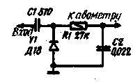
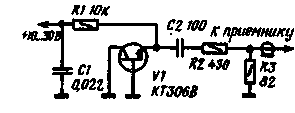
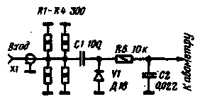
The noise generator circuit is shown in fig. 5. The source of noise is the emitter junction of the transistor V1, operating in reverse voltage breakdown mode. The intensity of the generated noise is several hundred kTo. This allows you to add an attenuator on resistors R2, R3 with an attenuation coefficient of about 13 dB to improve the matching of the probe with the receiver input. The probe is collected in a small box. During installation, special attention should be paid to the minimum length of the terminals of the transistor V1, resistors R2, R3 and capacitor C2. Even better results are obtained if a GA402 germanium microwave diode is used in the noise generator. It has a lower capacitance and lead inductance. The establishment of such a probe is reduced to setting the resistor R1 current through the diode within 1 ... 3 mA. For stable operation, it is desirable that the voltage of the power source is 2 ... 3 times higher than the voltage at which the breakdown of the diode begins. Using a probe, you can easily tune the receive path to maximum gain. To do this, it is necessary to connect an avometer to the output of the main receiver in the AC voltage measurement mode, and then by adjusting the circuits and selecting interstage connections to achieve the maximum readings of the device. The bandwidth of the receiving path of the transverter is also easy to determine by reducing the readings of the avometer when detuning the base receiver. The band is mainly determined by the parameters of the L16C43L17C45 filter, as well as the quality factor of the loaded circuit L18C50. The band can be expanded by increasing the capacitance of the capacitor C44 and reducing the division factor of the capacitive divider C51C52. The final adjustment is made using a measuring noise generator or while listening to signals received from the air. It should also be noted that the self-excitation of the RF amplifier when the antenna or its equivalent is turned off is not a sign of incorrect tuning of the receiving path. When establishing a transmission path, the operating modes of the transistors are first set to direct current. By selecting the resistor R10, the voltage at the collector of the transistor V4 is 4-7 V, which corresponds to a current of 10 mA. Resistor R8 sets the operating mode of the transistor V3 (there should be a voltage of +9 V on its collector). When adjusting the initial current of the terminal and terminal transistors, it is better to measure the DC voltage on the collector relative to the "positive" wire. The voltage drop across the resistor R4 should be 4 V, and across R1-0,2 V. After that, temporarily turn off the power from transistors VI and V2 and proceed to tune the resonant circuits. The initial setting is made in the absence of a signal with a frequency of 21 MHz (28 MHz). The resonant circuits L8C15, L7C14 to L6C10 are tuned to the local oscillator frequency, i.e., to a frequency of 123 MHz (116 MHz), using a high-frequency probe connected in turn to these circuits. Then, a signal with a frequency of 21,2 MHz (28,2 MHz) is applied to the mixer input. The signal amplitude is increased until a noticeable decrease in the collector current of transistor V4 begins. At the same time adjust the circuit L14C35C37. The local oscillator signal at the mixer output should then decrease somewhat. Then the high-frequency probe is weakly connected to the resonator L8 and, by rotating the axis of the trimmer capacitor C15 (in the direction of decreasing capacitance), the nearest voltage maximum is found (it should correspond to a frequency of 144,2 MHz). Then, the L7C14 and L6C10 circuits are sequentially tuned to the same frequency. Lastly, the last two cascades of the transmitting path are adjusted. To avoid failure of the transistor V1, the transmission path must be connected to a load corresponding to the impedance of the feeder. If it is planned to use a feeder with a wave impedance of 75 ohms, then four MLT-2 resistors connected in parallel with a resistance of 300 ohms can be used as a load, if 50 ohms, then six such resistors. The load (Fig. 6) is equipped with a diode detector that allows you to control the output power of the transmitter.
The load resistors and the detector will be placed in a small metal box equipped with a high-frequency connector. Resistors R1-R4 are arranged in a star pattern around the connector. They must have a minimum lead length. If the detector is provided with its own pointer indicator, then an autonomous device will be obtained - the simplest power meter. After connecting the load and supplying voltage to the last two stages, they begin to tune the L4C6 circuit, achieving the maximum collector current of the transistor V1. Before this, the transistor V1 must be connected to the load as much as possible, i.e., the capacitor C1 should have the maximum capacitance, and the capacitor C2 should have the minimum capacitance. The collector current of the transistor V1 can reach a value of 500 mA or more. If the excitation is insufficient, then it is useful to once again adjust all the preliminary stages, as well as slightly reduce the capacitance of the capacitors C5 and C7. The output circuit is adjusted to the maximum reading of the power indicator. It should be taken into account that the larger the capacitance of the capacitor C2, the weaker the connection with the load. With a weak connection and a maximum excitation level, the transistor can go into a highly overvoltage mode, in which there is a danger of the transistor failing. Therefore, such modes of operation should be avoided. Author: S Zhutyaev (UW3FI), Moscow; Publication: N. Bolshakov, rf.atnn.ru
Machine for thinning flowers in gardens
02.05.2024 Advanced Infrared Microscope
02.05.2024 Air trap for insects
01.05.2024
▪ Ancient Roman concrete can be restored ▪ Waterproof AC-DC adapters Mean Well OWA-90E ▪ The use of sodium bismuthate will accelerate the development of electronics
▪ section of the site Civil radio communications. Article selection ▪ Embrace of Morpheus article. Popular expression ▪ article How did hedgehogs shape McDonald's ice cream cups? Detailed answer ▪ article Main rotor of an autogyro. Personal transport ▪ article Gas pipe detector. Encyclopedia of radio electronics and electrical engineering ▪ article The Secret of the Seven. Focus Secret
Home page | Library | Articles | Website map | Site Reviews
www.diagram.com.ua |

 Leave your comment on this article: