|
|


 Arabic
 Bengali
 Chinese
 English
 French
 German
 Hebrew
 Hindi
Hindi Italian
 Japanese
 Korean
 Malay
Malay Polish
 Portuguese
 Spanish
 Turkish
 Ukrainian
 Vietnamese
|
ENCYCLOPEDIA OF RADIO ELECTRONICS AND ELECTRICAL ENGINEERING Electronic power switch-fuse. Encyclopedia of radio electronics and electrical engineering
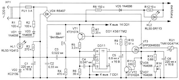
Encyclopedia of radio electronics and electrical engineering / Clocks, timers, relays, load switches The proposed device is designed to turn on (off) and protect against overcurrent of various radio-electronic equipment, lighting and other devices with mains power. A powerful field switching transistor is used as a switching element. Currently, part of the electronic equipment - TVs, DVD players, some equipment for computers - does not have a special mains power switch and is constantly connected to the network, although this is not necessary. Along with the fact that electricity is wasted in this case, the probability of its failure due to emergency situations in the network increases. The proposed device can be used not only to turn on such equipment, but also to protect against overcurrent.
The load is switched by a powerful field switching transistor VT3, which is included in the diagonal of the diode rectifier bridge VD4. Resistors R13, R14 are installed in the source circuit, which act as a current sensor. Diodes VD6, VD7 limit the voltage on them, and the capacitor C6 suppresses impulse noise. Varistor RU1 protects the transistor VT3 from breakdown by voltage surges that occur in the network when switching an inductive load. The switching transistor control unit is assembled on transistors VT1, VT2 and a D-trigger DD1.1, which is included as a frequency divider by two. The node is powered by a rectifier on diodes VD1, VD3 with quenching resistors R1, R2 and a parametric voltage stabilizer on a zener diode VD2, capacitor C1 is smoothing. LED HL1 indicates the presence of mains voltage at the input of the device. If the load power is turned off, the current through the HL1 LED increases, so the brightness of its glow increases. The load is connected in series with the diode bridge VD4, it is protected from overload, like the device itself, by the fusible insert FU1. LED HL2 indicates the presence of mains voltage at the load. Resistor R12, shunting the HL2 LED, eliminates its weak glow, which can occur due to the reverse current of the field-effect transistor VT3 and the current through the varistor RU1. After applying the mains voltage to the D-flip-flop DD1.1, the supply voltage is supplied. Capacitor C5 is designed to generate a pulse to set the D-flip-flop DD1.1 to the zero state - with a low logic level voltage at the direct output (pin 1 DD1.1). It happens like this. At the moment the supply voltage is applied, the capacitor C5 is charged, the transistor VT1 opens and a high level is applied to the input R (pin 4) of the D-flip-flop. The field effect transistor VT3 is closed, and the mains voltage is not supplied to the load. With a short press on the SB1 button, a high voltage level will go to the counting input C of the D-flip-flop, and it will switch to a state with a high level at the direct output. The channel resistance of the transistor VT3 will decrease to fractions of an ohm, and the supply voltage will be supplied to the load. Subsequent pressing of the SB1 button will cause the D-flip-flop to switch to a low level state at the direct output, the transistor VT3 will close, and the load will be de-energized. With an increase in the current consumed by the load, the voltage across the resistors R13, R14 increases, and when it reaches 0,55 ... 0,6 V, the transistor VT2, followed by VT1, will start to open, a high level, and it will switch to a low level state at the direct output, so the transistor VT3 will close and the load will be de-energized. The protection operation current can be set by the resistor R14 in the range of 0,08 ... 0,36 A. Since the transistors VT1, VT2 are closed in the steady state, and the D-trigger consumes a small current, after the mains voltage is turned off, the capacitor C1 can retain a charge for a long time. Resistor R3 serves to discharge it. This can be useful if it is necessary that during a long (minute or more) loss of mains voltage, the load is disconnected. Most of the parts are placed on a printed circuit board made of one-sided foil fiberglass, the drawing of which is shown in the figure.
It is designed for the use of fixed resistors MLT, S1-4, S2-23 (wire variable resistor PPB-Za is installed on the wall of a plastic case), oxide capacitors K50-35 or imported, the rest - K10-17. We will replace the TNR10G471K varistor with FNR-10K471, FNR-07K471, the KS213B zener diode with KS213A, 1N4743A, the RS407 diode bridge with KBL08, KBL10, the 1N4006 diodes with 1N4007. LEDs can be used with a constant, but different glow color (HL1 - green, HL2 - red) from the L-53, KIPD40 series. The KT3107A transistor can be replaced by any of the KT3107, KT361, KT349 series, the KT3102A transistor - by any of the KT315, KI3102, KT342 series, but you need to pay attention to the difference in the pinouts of the transistors. The SPP20N60S5 field effect transistor has an open channel resistance of 0,19 ohms, a maximum drain-source voltage of 600 V, a maximum drain current of 20 A, and a pulsed one - up to 40 A. Its closest analogues are IRFP460, STW20NB50, but you can also install a more powerful one - SPW47N60C3, having an open channel resistance of 0,07 ohms and a maximum drain current of 47 A. When conducting experiments or for operating a device with a low-power load, transistors IRF840 or the KP707, KP753 series are suitable. Button SB1 - any small-sized button with a long plastic pusher, for example, TD06-XEX, TD06-XBT. With the values of resistors R13, R14 indicated in the diagram, a load with a power of up to 75 W can be connected to the device. Therefore, when connecting to the device, for example, an incandescent lamp with a power of 100 ... 150 W, the current protection will work and prevent it from turning on. To control a more powerful load, it is necessary to reduce the resistance of the resistor R13. The amplitude value of the protection operation current can be found from the expression Ia = (0,55...0,6)/(R13+R14). Most electrical and radio devices, when connected to the network, consume the so-called starting current, which is several times higher than the rated current. In order for the current protection not to work, it is necessary to install an oxide capacitor (with a positive terminal to the emitter) with a capacity of 1 ... 47 μF in parallel with the emitter junction of the transistor VT100. A seat for this capacitor is provided on the board. The starting current of devices with switching power supplies that have high-capacity capacitors at the input can be reduced by connecting a wire resistor with a resistance of 3,3 ... 5,6 Ohm and a power of 5-10 W in series with the load, for example, C5-37, C5- 16. If this is not done, then relatively low-current field-effect transistors (IRF840, etc.) may be damaged already when the load is turned on for the first time (TV, printer, monitor) Author: A.L. Butov, p. Kurba, Yaroslavl region; Publication: cxem.net
Machine for thinning flowers in gardens
02.05.2024 Advanced Infrared Microscope
02.05.2024 Air trap for insects
01.05.2024
▪ Rheumatics and athletes - in the cold ▪ CFexpress Type B memory cards ▪ Duracell Powercheck technology detects battery charge ▪ Hybrid trash can with slot machine
▪ section of the site Standard instructions for labor protection (TOI). Selection of articles ▪ article Coffins burnt. Popular expression ▪ article Which court considers Wikipedia a reliable source of information? Detailed answer ▪ article Chemical analysis laboratory assistant. Job description ▪ article Power supply for any design. Encyclopedia of radio electronics and electrical engineering ▪ article Four aces. Focus Secret
Home page | Library | Articles | Website map | Site Reviews
www.diagram.com.ua |


 Leave your comment on this article: