|
|


 Arabic
 Bengali
 Chinese
 English
 French
 German
 Hebrew
 Hindi
Hindi Italian
 Japanese
 Korean
 Malay
Malay Polish
 Portuguese
 Spanish
 Turkish
 Ukrainian
 Vietnamese
|
ENCYCLOPEDIA OF RADIO ELECTRONICS AND ELECTRICAL ENGINEERING Zero detector. Encyclopedia of radio electronics and electrical engineering
Encyclopedia of radio electronics and electrical engineering / Indicators, detectors The proposed device generates short pulses (0,3-1 ms) relative to zero (zero crossing) of the mains voltage sine wave. The circuit output is galvanically isolated from the mains. The device can be used to synchronize power thyristor blocks, as a 100 Hz (50 Hz) frequency generator, to quickly detect mains voltage failure, etc. It also allows you to generate a pulse starting at the beginning of the phase (phase detector). The scheme of the device is shown in Fig.1.
Resistor R1 limits the current consumption to 3 mA. The presence of this high-resistance resistor together with the VD7 zener diode makes it possible to use low-voltage capacitors, diodes and transistors in the circuit. The diode bridge VD1 ... VD4 converts the alternating voltage into a unipolar, pulsating one. Through the diode VD5, this voltage is supplied to the power circuit of the circuit, the zener diode VD7 limits the voltage, and the capacitor C2 smoothes the ripple. The capacitance of the capacitor C2 in the power circuit is selected large (22 μF) when the device is used as a phase detector (otherwise the pulse at the top will be "blurred"). If the slope of the pulse is not critical, as well as in the zero detector circuit, the capacitance C2 can be reduced to 0,22 μF. With the specified capacitance C2, the time between turning on the device in the network and the appearance of the first pulse is about 150 ... 200 ms. At the same time, a pulsating voltage through the resistor R2 is applied to the base of the transistor VT1, periodically opening it, and short pulses with a duration of 1 ... 3 ms appear on the VT0,2 collector (at point X0,3). With the zero detector option, a jumper is switched on between points X3 and X4. Then the resistors R4 and R5 are connected in parallel, and the transistor VT2 is turned off. Rectangular pulses through the decoupling capacitor C1 are fed to the base of the composite transistor VT3-VT4. Since the pulses on the VT1 collector are short, the capacitor C1 does not have time to fully charge, and with the specified capacitance, the pulse length is not limited. Capacitor C1 is discharged through diode VD6 when the pulse falls. The composite transistor, opening for 0,2 ... 0,3 ms, turns on the LED of the optocoupler VU1. The current through the LED is selected approximately 12 ... 15 mA. The LED switches the phototransistor, from which the output signal is taken, galvanically isolated from the network. The contacts X9 and X8 are supplied with supply voltage (5 ..10 V) from the circuit where the detector signal is used. In this case, the phototransistor is connected according to the common collector circuit, the output is contact X7 (Out. 1). With a resistance R7 of 100 Yum, the output pulses have gentle fronts and a duration of about 1 ms. and with a resistance of 10 kOhm - 0,3 ms with steep fronts. If it is necessary to have an inverted signal, "+" power supply is applied to contact X6, "-" - to X7. resistor R7 is connected between X6 and X9, and the signal is removed from the output X9 (Out.0). In the version of the phase detector, a jumper is installed between contacts X3 and X5. Pulses from the collector VT1 are fed to the base VT2. On its collector, the signal is inverted, i.e. missing for 0,2.-0.3 ms. Through C1, pulses from the VT2 collector arrive, as in the previous version. on a composite transistor VT3-VT4. Time diagrams of device operation for both options are shown in Fig.2.
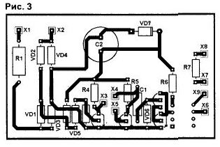
Any low-power low-voltage transistors and diodes can be used in the device. Zener diode - with a stabilization voltage of 9 ... 15 V The type of optocoupler is also not critical - any with the necessary insulation voltage (at least 300 V). The resistor values are not critical (47 ... 200 kOhm), but with a decrease in the resistance R1, its power dissipation increases, which must be taken into account. The current consumption of the device is about 2 mA, but it can be reduced by increasing the resistance R1. The detector is assembled on a printed circuit board, the drawing of which is shown in Fig.3.
Author: V. Khvostik, v. Tsaredarovka, Kharkiv region.
Machine for thinning flowers in gardens
02.05.2024 Advanced Infrared Microscope
02.05.2024 Air trap for insects
01.05.2024
▪ ADAV400 multi-channel audio codec ▪ Newsweek magazine stops publishing in print
▪ section of the site Grounding and grounding. Selection of articles ▪ article Pluck flowers of pleasure. Popular expression ▪ article Who was on the first Apple logo? Detailed answer ▪ article Foreign bodies of the eye. Health care ▪ article SAMSUNG flash memory chips. Encyclopedia of radio electronics and electrical engineering
Home page | Library | Articles | Website map | Site Reviews
www.diagram.com.ua |


 Leave your comment on this article: