|
|


 Arabic
 Bengali
 Chinese
 English
 French
 German
 Hebrew
 Hindi
Hindi Italian
 Japanese
 Korean
 Malay
Malay Polish
 Portuguese
 Spanish
 Turkish
 Ukrainian
 Vietnamese
|
ENCYCLOPEDIA OF RADIO ELECTRONICS AND ELECTRICAL ENGINEERING Transistor switches. Encyclopedia of radio electronics and electrical engineering
Encyclopedia of radio electronics and electrical engineering / Clocks, timers, relays, load switches The main purpose of transistor switches, the circuits of which are offered to the attention of readers, is to turn on and off the DC load. In addition, it can perform additional functions, for example, indicate its status, automatically turn off the load when the battery is discharged to the maximum allowable value or by a signal from temperature, light sensors, etc. A switch can be made based on several switches. Switching of current is carried out by the transistor, and control is carried out by one simple button with contact on closing. Each press of the button reverses the state of the switch. A description of a similar switch was given in [1], but there two buttons were used for control. The advantages of the proposed switches include non-contact connection of the load, practically no current consumption in the off state, accessible elements and the possibility of using a small-sized button that takes up little space on the instrument panel. Disadvantages - own current consumption (several milliamps) in the on state, voltage drop across the transistor (fractions of a volt), the need to take measures to protect a reliable contact in the input circuit from impulse noise (it can spontaneously turn off with a short-term contact failure). The switch circuit is shown in fig. 1. The principle of its operation is based on the fact that for an open silicon transistor, the voltage at the base-emitter junction of the transistor is 0,5 ... 0,7 V, and the collector-emitter saturation voltage can be 0,2 ... 0,3 Q. In fact, this device is a trigger on transistors with different structures, controlled by one button. After applying the supply voltage, both transistors are closed, and the capacitor C1 is discharged. When the SB1 button is pressed, the charging current of the capacitor C1 opens the transistor VT1, and the transistor VT2 opens after it. When the button is released, the transistors remain on, the supply voltage (minus the voltage drop across the transistor VT1) is supplied to the load and the capacitor C1 will continue to charge. It will charge up to a voltage slightly higher than the base voltage of this transistor, since the collector-emitter saturation voltage is less than the base-emitter voltage.
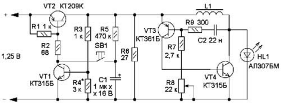
Therefore, the next time you press the button, the base-emitter voltage on transistor VT1 will be insufficient to keep it open and it will close. Next, the transistor VT2 will close, and the load will be de-energized. Capacitor C1 will discharge through the load and resistors R3-R5, and the switch will return to its original state. The maximum collector current of the transistor VT1 Iк depends on the current transfer coefficient h21Э and base current Iб: Iк = Iб h21Э. For the ratings and types of elements indicated on the diagram, this current is 100 ... 150 mA. For the breaker to work properly, the current drawn by the load must be less than this value. This switch has two features. If there is a short circuit at the output of the switch, after a short press on the SB1 button, the transistors will open for a short time and then, after charging the capacitor C1, they will close. When the output voltage decreases to about 1 V (depending on the resistances of resistors R3 and R4), the transistors will also close, i.e., the load will be de-energized. The second property of the switch can be used to build a discharge device for individual Ni-Cd or Ni-Mh batteries up to 1 V before compiling them into a battery and further general charging. The scheme of the device is shown in fig. 2. The switch on transistors VT1, VT2 connects a discharge resistor R6 to the battery, in parallel with which a voltage converter [2] is connected, assembled on transistors VT3, VT4, which feeds the HL1 LED. The LED indicates the status of the discharging process and is an additional load on the battery. Resistor R8 can change the brightness of the LED, as a result of which the current consumed by it changes. In this way, the discharge current can be adjusted. As the battery discharges, the voltage at the input of the switch decreases, as well as at the base of the transistor VT2. The divider resistors in the base circuit of this transistor are selected so that when the input voltage is 1 V, the voltage at the base will decrease so much that the transistor VT2 closes, and after it the transistor VT1 - the discharge will stop. With the ratings of the elements indicated in the diagram, the interval for adjusting the discharge current is 40 ... 90 mA. If the resistor R6 is excluded, the discharge current can be changed in the range from 10 to 50 mA. When using a super-bright LED, this device can be used to build a flashlight with battery protection from deep discharge.
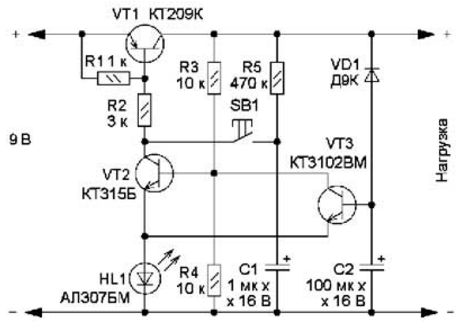
On fig. 3 shows another application of the switch - a timer. It was used by me in a portable device - a tester of oxide capacitors. The HL1 LED is additionally introduced into the circuit, which indicates the state of the device. After switching on, the LED lights up and the capacitor C2 begins to be charged by the reverse current of the diode VD1. At a certain voltage, transistor VT3 will open on it, which will short-circuit the emitter junction of transistor VT2, which will turn off the device (the LED will turn off). Capacitor C2 will quickly discharge through the diode VD1, resistors R3, R4 and the switch will return to its original state. The exposure time depends on the capacitance of the capacitor C2 and the reverse current of the diode. With the elements indicated in the diagram, it is about 2 minutes. If we install a photoresistor, a thermistor (or other sensors) instead of capacitor C2, and a resistor instead of a diode, we get a device that will turn off when the light, temperature, etc. changes.
If there are large capacitors in the load, the circuit breaker may not turn on (depending on their capacitance). A diagram of a device devoid of this drawback is shown in Fig. 4. Another transistor VT1 has been added, which performs the function of a key, and two other transistors control this key, which eliminates the effect of the load on the operation of the switch. But at the same time, the property will be lost not to turn on if there is a short circuit in the load circuit. The LED performs a similar function. With the ratings of the parts indicated in the diagram, the base current of the transistor VT1 is about 3 mA.
Several transistors KT209K and KT209V were tested as a key. They had base current transfer ratios from 140 to 170. At a load current of 120 mA, the voltage drop across the transistors was 120...200 mV. At a current of 160 mA - 0,5 ... 2,2 V. The use of a composite transistor KT973B as a key made it possible to significantly increase the permissible load current, but the voltage drop across it was 750 ... 850 mV, and at a current of 300 mA the transistor is weakly warmed up. In the off state, the current consumption is so small that it was not possible to measure it with the DT830B multimeter. At the same time, the transistors were not preliminarily selected according to any parameters. On fig. 5 shows a diagram of a three-channel dependent switch. It combines three switches, but if necessary, their number can be increased. A short press on any of the buttons will turn on the corresponding switch and connect the corresponding load to the power source. If you press any other button, the corresponding switch will turn on, and the previous one will turn off. Pressing the next button will turn on the next switch, and the previous one will turn off again. When you press the same button again, the last working switch will turn off and the device will return to its original state - all loads will be de-energized. The switching mode is provided by resistor R5. When a switch is turned on, the voltage across this resistor increases, which leads to the closing of the previously switched on switch. The resistance of this resistor depends on the current consumed by the switches themselves, in this case its value is about 3 mA. Elements VD1, R3 and C2 provide the passage of the discharge current of capacitors C3, C5 and C7. Through the resistor R3, the capacitor C2 discharges in the pauses between pressing the button. If this circuit is eliminated, only the on and switch modes remain. Replacing the resistor R5 with a jumper wire, we get three independently operating devices.
The switch was supposed to be used in the switch of television antennas with amplifiers, but with the advent of cable television, the need for it disappeared, and the project was not put into practice. Switches can use many different types of transistors, but they must meet certain requirements. First, they must all be silicon. Secondly, transistors that switch the load current must have a saturation voltage Uto us not more than 0,2 ... 0,3 V, the maximum allowable collector current Iк max must be several times greater than the switched current, and the current transfer coefficient h21э sufficient so that at a given base current, the transistor is in saturation mode. Of the transistors I have, the transistors of the KT209 and KT502 series have proven themselves well, and the KT3107 and KT361 series are somewhat worse. The resistance of the resistors can be changed over a wide range. If greater efficiency is required and indication of the switch status is not needed, the LED is not installed, and the resistor in the VT3 collector circuit (see Fig. 4) can be increased to 100 kOhm or more, but it must be taken into account that this will reduce the base current of the VT2 transistor and the maximum load current. Transistor VT3 (see Fig. 3) must have a current transfer coefficient h21э more than 100. The resistance of the resistor R5 in the charging circuit of the capacitor C1 (see Fig. 1) and similar ones in other circuits can be in the range of 100 ... 470 kOhm. Capacitor C1 (see Fig. 1) and similar ones in other circuits should be with a low leakage current, it is desirable to use the K53 oxide semiconductor series, but oxide can also be used, while the resistance of the resistor R5 should be no more than 100 kOhm. With an increase in the capacitance of this capacitor, the performance will decrease (the time after which the device can be turned off after being turned on), and if it is reduced, the clarity of operation will decrease. Capacitor C2 (see Fig. 3) - only oxide-semiconductor. Buttons - any small-sized with self-return. Coil L1 of the converter (see Fig. 2) is used from the linearity regulator of the lines of a black-and-white TV, the converter also works well with a choke on the W-shaped magnetic circuit from the CFL. You can also use the recommendations given in [2]. Diode VD1 (see Fig. 5) can be any low-power, both silicon and germanium. Diode VD1 (see Fig. 3) must be germanium. Adjustments require devices, the diagrams of which are shown in fig. 2 and fig. 5, the rest do not need to be adjusted if there are no special requirements and all the details are in good order. To set up a discharge device (see Fig. 2), you will need a power supply with an adjustable output voltage. First of all, instead of the resistor R4, a variable resistor with a resistance of 4,7 kOhm is temporarily installed (to the maximum resistance). The power source is connected, having previously set a voltage of 1,25 V at its output. The discharge device is turned on by pressing the button and the required discharge current is set using resistor R8. After that, a voltage of 1 V is set at the output of the power source, and with the help of an additional variable resistor, the device is turned off. After that, you need to check the turn-off voltage several times. To do this, it is necessary to increase the voltage at the output of the power supply to 1,25 V, turn on the device, then it is necessary to gradually reduce the voltage to 1 V, observing the moment of switching off. Then the introduced part of the additional variable resistor is measured and replaced with a constant one with the same resistance. In all other devices, you can also implement a similar shutdown function when the input voltage drops. Adjustment is done in a similar way. At the same time, the fact that near the turn-off point, the transistors begin to close smoothly and the current in the load will also gradually decrease. If there is a radio receiver as a load, then this will manifest itself as a decrease in volume. Perhaps the recommendations described in [1] will help solve this problem. Establishing a switch (see Fig. 5) is reduced to a temporary replacement of fixed resistors R3 and R5 with variables with a resistance of 2 ... 3 times more. By successively pressing the buttons, using the resistor R5, they achieve reliable operation. After that, by repeatedly pressing the same button with the help of resistor R3, a reliable shutdown is achieved. Then the variable resistors are replaced by constant ones, as mentioned above. To increase noise immunity, ceramic capacitors with a capacity of several nanofarads must be installed in parallel with resistors R7, R13 and R19. Literature
Author: V. Bulatov
Machine for thinning flowers in gardens
02.05.2024 Advanced Infrared Microscope
02.05.2024 Air trap for insects
01.05.2024
▪ Robomobiles for highway construction ▪ Named the best time for lunch ▪ Portable solar charging for electric vehicles from Volvo ▪ The world's first solar road
▪ section of the site Your stories. Article selection ▪ article The luxury of your own opinion. Popular expression ▪ article Why is the name Silicon Valley essentially wrong? Detailed answer ▪ article Asphodel. Legends, cultivation, methods of application
Home page | Library | Articles | Website map | Site Reviews
www.diagram.com.ua |


 Leave your comment on this article: