Electronic fuse. Encyclopedia of radio electronics and electrical engineering

Encyclopedia of radio electronics and electrical engineering / Radio amateur designer
 Comments on the article
As you know, there are many different current sources that do not provide protection against emergency current overloads - these are almost all galvanic cells and batteries, most batteries and batteries from them, network power supplies assembled according to the simplest scheme, etc. no less often, such sources are used to power the load for a long time without the supervision of an operator.
If for one reason or another there is a significant increase in the current consumed by the load, this will naturally lead to overheating of such a source and its failure, sometimes with very serious consequences. The device described below is intended for automatic disconnection of the load from the DC source in the event of an overload in its circuit and for light indication of an emergency condition. This two-pole, like a fuse, is included in the break in the positive wire of the load circuit.
The electronic fuse (Fig. 1) consists of a powerful composite switching element based on VT4VT3 transistors, a current-measuring resistor R2, a transistor analog of the VT1VT2 dinistor and a shunt transistor VT5.
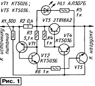
When the power source is turned on, the composite transistor VT4VT3 opens with a current flowing through the resistor R1 and the emitter junction of the transistor VT4. The remaining transistors remain closed. The rated voltage is supplied to the load, the rated current flows through it.
When an overload occurs, the voltage drop across the current-measuring resistor becomes sufficient to open the analog of the dinistor. Following it, the transistor VT5 opens and shunts the emitter junction of the transistor VT4. As a result, transistors VT4 and VT3 are closed, disconnecting the load from the power source. The load current decreases sharply, but the analog of the dinistor remains open.
The fuse can remain in this state indefinitely. A residual current flows through the load, determined by the resistance of the resistor R1, i.e., ten times less than the nominal one. The voltage drop across the closed transistor VT3 turns on the LED HL1 "Crash".
In order to resume the operation of the load in the nominal mode after the elimination of the cause that caused the overload, it is necessary to either turn off the power source for a short time or disconnect the load.
With the ratings of parts indicated in the diagram, the fuse has the following Features:
- Rated supply voltage. AT 12
- Rated load current, A ...... 1
- Operation current, A ...... 1,2
- Residual voltage on the load after the fuse tripped, V......1,2
- Voltage drop across the fuse in nominal mode, mV......750
The advantage of this fuse, in comparison with that described in [1], is a more reliable closing of the switching element (since the voltage across the open and saturated transistor VT5 is significantly less than on the open trinistor VS1 in [1]. In addition, the voltage drop across the switching element of the considered the fuse is much smaller than that of the compared one; this is achieved by using transistors of various structures in it [2].
The device is easily placed on a 45x45 mm printed circuit board (Fig. 2). Transistor VT3 is best used as indicated in the diagram. Attempts to replace it with other powerful transistors led to an increase in the voltage drop across the fuse.

It is necessary to include a fuse in the protected circuit in a strictly defined polarity. This requires the application of appropriate marking of its conclusions.
Literature
- Esaulov N. Adjustable electronic fuse. - Radio, 1988, No. 5, p. 31,32.
- Golovatsky V. A. et al. Sources of secondary power supply. - M.: Radio and communication, 1990, p. 86.
Author: O. Sidorovich, Lviv, Ukraine
 See other articles Section Radio amateur designer.
Read and write useful comments on this article.
<< Back
 Latest news of science and technology, new electronics:
A New Way to Control and Manipulate Optical Signals
05.05.2024
The modern world of science and technology is developing rapidly, and every day new methods and technologies appear that open up new prospects for us in various fields. One such innovation is the development by German scientists of a new way to control optical signals, which could lead to significant progress in the field of photonics. Recent research has allowed German scientists to create a tunable waveplate inside a fused silica waveguide. This method, based on the use of a liquid crystal layer, allows one to effectively change the polarization of light passing through a waveguide. This technological breakthrough opens up new prospects for the development of compact and efficient photonic devices capable of processing large volumes of data. The electro-optical control of polarization provided by the new method could provide the basis for a new class of integrated photonic devices. This opens up great opportunities for ... >>
Primium Seneca keyboard
05.05.2024
Keyboards are an integral part of our daily computer work. However, one of the main problems that users face is noise, especially in the case of premium models. But with the new Seneca keyboard from Norbauer & Co, that may change. Seneca is not just a keyboard, it is the result of five years of development work to create the ideal device. Every aspect of this keyboard, from acoustic properties to mechanical characteristics, has been carefully considered and balanced. One of the key features of Seneca is its silent stabilizers, which solve the noise problem common to many keyboards. In addition, the keyboard supports various key widths, making it convenient for any user. Although Seneca is not yet available for purchase, it is scheduled for release in late summer. Norbauer & Co's Seneca represents new standards in keyboard design. Her ... >>
The world's tallest astronomical observatory opened
04.05.2024
Exploring space and its mysteries is a task that attracts the attention of astronomers from all over the world. In the fresh air of the high mountains, far from city light pollution, the stars and planets reveal their secrets with greater clarity. A new page is opening in the history of astronomy with the opening of the world's highest astronomical observatory - the Atacama Observatory of the University of Tokyo. The Atacama Observatory, located at an altitude of 5640 meters above sea level, opens up new opportunities for astronomers in the study of space. This site has become the highest location for a ground-based telescope, providing researchers with a unique tool for studying infrared waves in the Universe. Although the high altitude location provides clearer skies and less interference from the atmosphere, building an observatory on a high mountain poses enormous difficulties and challenges. However, despite the difficulties, the new observatory opens up broad research prospects for astronomers. ... >>
| Random news from the Archive Crystal of electrons
16.07.2021
A team of researchers from ETH Zurich has observed a Winger crystal for the first time in history. The discovery is described as nothing more than the Holy Grail in condensed matter physics.
In 1934, Eugene Wigner suggested that electrons in a material could theoretically arrange themselves in regular and crystalline structures due to mutual electrical repulsion. For almost 90 years, the prediction existed in the form of a theory, and only recently was it experimentally proven. Swiss scientists were able to actually fix a crystal consisting of only electrons.
The main problem that accompanied all previous attempts to prove this theory was the need for extremely low temperatures and a small number of free electrons in the material. In the course of new experiments, it was possible to create a layer of molybdenum diselenide just one atom thick. This made the electrons move in only one plane, and their number depended on the voltage applied to two transparent graphene electrodes, between which there was a semiconductor.
The material was cooled to several degrees above absolute zero, and the electron separation did not exceed 20 nanometers, which made it possible to study them with a microscope. The researchers achieved that the regular arrangement of electrons became visible by using light of a certain frequency to excite excitons in the semiconductor layer, which made it possible to see the Wigner crystal.
|
Other interesting news:
▪ On the benefits of family scandals
▪ Origins of human speech found
▪ Want to lose weight - sniff vanilla
▪ How to beat smartphone addiction
▪ Antimatter falls down like normal matter
News feed of science and technology, new electronics
 Interesting materials of the Free Technical Library:
▪ site section Color and music installations. Selection of articles
▪ article A man in his place. Popular expression
▪ article Why does water flow from a spring? Detailed answer
▪ article by Alessandro Volta. Biography of a scientist
▪ article Indicator of beta and gamma radiation. Encyclopedia of radio electronics and electrical engineering
▪ article Phonograph record against gravity. Focus Secret
Leave your comment on this article:
 All languages of this page
Home page | Library | Articles | Website map | Site Reviews

www.diagram.com.ua
2000-2024


 Arabic
 Bengali
 Chinese
 English
 French
 German
 Hebrew
 Hindi
Hindi Italian
 Japanese
 Korean
 Malay
Malay Polish
 Portuguese
 Spanish
 Turkish
 Ukrainian
 Vietnamese