|
|


 Arabic
 Bengali
 Chinese
 English
 French
 German
 Hebrew
 Hindi
Hindi Italian
 Japanese
 Korean
 Malay
Malay Polish
 Portuguese
 Spanish
 Turkish
 Ukrainian
 Vietnamese
|
ENCYCLOPEDIA OF RADIO ELECTRONICS AND ELECTRICAL ENGINEERING Thickness gauge. Encyclopedia of radio electronics and electrical engineering
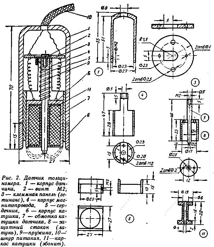
Encyclopedia of radio electronics and electrical engineering / Measuring technology Measurement of the thickness of metal coatings on a ferromagnetic basis is carried out during the control of finished products, in the process of galvanic coating, as well as in determining the degree of wear of a particular part. Existing instruments for measuring coating thickness are quite complex and cumbersome. At the Department of Automation, Telemechanics and Electronics of the Azerbaijan Institute of Oil and Chemistry named after. M. A. Azizbekov developed a portable gauge for the thickness of non-magnetic coatings on a ferromagnetic base. The device, named by the author ITP-63, makes it possible to determine the thickness of a non-magnetic coating under any production conditions without destroying the coating itself and the part. The thickness of the coating layer, which can be measured with this instrument, ranges from 0 to 100 microns. With careful adjustment of the device, it can measure films up to 500 microns thick. The device is extremely simple in design and can be easily repeated according to the description given in the article by medium-skilled radio amateurs. The device is powered from the AC mains, however, with minor modifications, it can be powered from built-in current sources. The device passed production tests and was demonstrated at the Exhibition of Achievements of the National Economy in Moscow. Thickness gauge type ITP-63 is designed to measure the thickness of the chromium coating layer on ferromagnetic bases. The principle of operation of the device, the scheme of which is shown in Fig. 1 is based on the change in the inductive reactance of the sensor L1 depending on the thickness of the chrome plating.
The sensor of the device is included in the shoulder of the bridge. When the thickness of the coatings (o) changes, the inductive resistance of the sensor L1 changes, the balance of the bridge is disturbed, and the M-24 device detects a change in current for 100 μA. The scale of the device is graduated in microns, so you can directly measure the thickness of the chrome coating. The thickness gauge was calibrated on special samples, the coating thickness of which was previously determined with a high accuracy micrometer. Obtaining two extreme points (zero and maximum) is carried out by changing the resistances R3 and R4. The calibration accuracy of the instrument strongly depends on the accuracy of the sample itself. The sensitivity of the thickness gauge is determined by the value of the selected supply voltage for each device (up to saturation of the sensor core and compensating device). As the voltage increases, the sensitivity increases. In addition, the greater the number of turns and the cross section of the core of the coils L1 and L2, the higher the sensitivity of the device. The sensitivity of the thickness gauge largely depends on the optimal value of the resistances R3, R4 and the capacitance of the capacitor C2. With the correct selection of these elements, the measurement limit can be increased to 500 microns. The design of the compensating device sensor is shown in fig. 2 and 3. Coils L1 and L2 each contain 800 turns of PEL-0,21 wire. The coils of the sensor and the compensating device are wound in bulk.
The indicated resistances R5 -R6 and thermistor type T8R (or TSh-1) are used to linearize the scale of the thickness gauge instrument. The linearity of the thickness gauge scale also depends on the characteristics of the thermistor and diodes included in the bridge arm. To stabilize the supply voltage, resistances R1, R2, silicon zener diodes of the D809 type and diodes of the D7D type connected in series with them were used.
The device is made in the form of a portable structure with a horizontal pointer and a remote sensor. The dimensions of the device are 210x150x70 mm. The weight of the device with the sensor is 2,1 kg. The contact area of the sensor with the measured object is 27x27 mm. The device is powered by AC 220 V, the measurement limit is from 0 - 100 microns. The total error of the thickness gauge does not exceed 4%. Literature:
Author: M. Aliyev; Publication: N. Bolshakov, rf.atnn.ru
Machine for thinning flowers in gardens
02.05.2024 Advanced Infrared Microscope
02.05.2024 Air trap for insects
01.05.2024
▪ Lextar PR88 infrared LED module ▪ Silicon Carbide Mass Production Plant ▪ Beam splitter roof for solar greenhouse
▪ section of the site House, household plots, hobbies. Article selection ▪ article Conflict of the good with the best. Popular expression ▪ How did Achilles, the greatest Greek hero of the Trojan War, die? Detailed answer ▪ article Moulder. Standard instruction on labor protection
Home page | Library | Articles | Website map | Site Reviews
www.diagram.com.ua |


 Leave your comment on this article: