|
|


 Arabic
 Bengali
 Chinese
 English
 French
 German
 Hebrew
 Hindi
Hindi Italian
 Japanese
 Korean
 Malay
Malay Polish
 Portuguese
 Spanish
 Turkish
 Ukrainian
 Vietnamese
|
ENCYCLOPEDIA OF RADIO ELECTRONICS AND ELECTRICAL ENGINEERING High power timer. Encyclopedia of radio electronics and electrical engineering
Encyclopedia of radio electronics and electrical engineering / Clocks, timers, relays, load switches As you know, a timer is a device designed to automatically connect an electronic device to or disconnect from a power source. It is traditionally subject to, for example, such requirements as small dimensions, power consumption and voltage drop on the control circuit. Traditionally, the load was switched on through high-current relay contacts. With the advent of powerful switching transistors, say, IRLR2905, the need for a relay has disappeared, which made it possible to significantly reduce the size of the timer. It is this transistor that is used in the timer, the circuit of which is shown in Fig. 1. It is capable of operating at a voltage of 7,5 V and switching a load that consumes current up to 30 A.
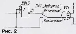
A voltage stabilizer is assembled on the DA1 microcircuit, a voltage comparator on the logic elements DD1.1, DD1.2, an inverter on the DD1.3, an electronic key on the transistor VT1. Capacitors C1 and C3 ensure stable operation of the voltage stabilizer, the parameters of the C2R1 chain set the timer operation time. Resistive divider R2R3 provides feedback in the voltage comparator and provides jump switching of the comparator from one stable state to another. Now about the operation of the device. After the supply voltage is applied, the charging of the capacitor C2 begins through the resistors R1 and R2. At the same time, at the input of the logic element DD1.1 there is a high logic level, and at the output - low. The field effect transistor VT1 is closed. As the capacitor C1 charges, the voltage at the input of the element DD1.1 decreases. When it reaches the switching threshold of the comparator, a voltage of about 5 V will appear at the gate of the transistor. The transistor will open, and the supply voltage will be supplied to the load connected to the sockets X1, X2. This is the load turn-on delay mode. To restart the timer, you must briefly press the button SB1 "Start". Capacitor C1 will be discharged, the countdown will start again. In order for the timer to work in the load off delay mode, it is necessary to disconnect the gate of the field-effect transistor from the output of the DD1.3 element and connect it to the output of the DD1.2 element. If the switch SA1 is introduced into the device (Fig. 2), the timer can work both in the turn-on delay mode and in the turn-off delay mode.
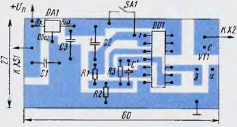
In the case of connecting an inductive load, the sockets should be shunted with a VD1 diode, and to reduce the likelihood of "bounce" when the load is turned on or off, capacitor C4 must be inserted. In addition to those indicated in the diagram, it is permissible to use the K561LA7 chip, and when changing the topology of the printed circuit board - 564LE5, K564LA7. The transistor can be any, highlighted in color, from the list given in the article "Powerful field-effect switching transistors from INTERNATIONAL RECTIFIER" in Radio, 2001, No. 5, p. 45. In this case, of course, the maximum current switched by the timer will be determined by the type of transistor used. The polar capacitor C2 should be a low-leakage surface-mount tantalum or K52 series, but then you will have to increase the size of the board. The remaining capacitors are K10-17. For a low-power load, the VD1 diode can be any of the KD102, KD103, KD105 series, and for a powerful load - KD109A-KD109V, KD212A, KD212B or similar. Resistors - MLT. С2-33, Р1-4, Р1-12, button and switch - any small-sized ones. With a load current of more than 1 A, the common power wire must be soldered as close as possible to the source of the transistor. If the current exceeds 8 A, the transistor should be installed (by soldering) on the heatsink. For a current of 30 A, its area should be 100 ... 150 cm2. When the supply voltage is 15 V or more, it is recommended to connect a 10 ... 20 Ohm resistor in series with the button to reduce the discharge current of the capacitor and protect the button contacts from burning. To increase the voltage at which the timer can operate to the operating voltage of the transistor, it is necessary to use the DA1 stabilizer with a large input voltage. The timer's own current consumption is determined mainly by the current of the stabilizer. Most of the details of the device are placed on a printed circuit board (Fig. 3) made of one-sided foil fiberglass.
Establishing a timer comes down to setting the required delay time by selecting resistor R1 and, if necessary, capacitor C2. For the ratings of these elements indicated in the diagram, the delay time was approximately 13 minutes. During tests of the timer layout at a current of 5 A, the voltage drop across the transistor was 0,1 V, and the power dissipated on it was 0,5 W, which indicates a good efficiency of the device. Author: I. Nechaev, Kursk
Machine for thinning flowers in gardens
02.05.2024 Advanced Infrared Microscope
02.05.2024 Air trap for insects
01.05.2024
▪ Stream S03 portable hard drives with USB 3.0 interface ▪ Portable devices harm the development of speech
▪ section of the site Palindromes. Article selection ▪ article You can't spill it with water. Popular expression ▪ article What is philosophy? Detailed answer ▪ article Self-oscillating multivibrator. Radio - for beginners
Home page | Library | Articles | Website map | Site Reviews
www.diagram.com.ua |


 Leave your comment on this article: