|
|


 Arabic
 Bengali
 Chinese
 English
 French
 German
 Hebrew
 Hindi
Hindi Italian
 Japanese
 Korean
 Malay
Malay Polish
 Portuguese
 Spanish
 Turkish
 Ukrainian
 Vietnamese
|
ENCYCLOPEDIA OF RADIO ELECTRONICS AND ELECTRICAL ENGINEERING Automobile laptop power supply on the KR1006VI1 timer. Encyclopedia of radio electronics and electrical engineering
Encyclopedia of radio electronics and electrical engineering / Automobile. Electronic devices To power a laptop, a voltage of about 19 V is required. To obtain it from the vehicle's on-board network, a step-up voltage converter is required. An example of the design of such a device on the KR1156EU5 microcircuit and the procedure for its calculation are described in the article by S. Muralev “Voltage converter for powering a laptop from a car battery” (Radio, 2008, No. 12, pp. 29-31). The proposed device is based on the KR1006VI1 timer chip. It differs from the prototype in a wider input voltage range and a high maximum output current. Main Specifications
The device diagram is shown in Fig. 1. The DA1 chip contains a generator of rectangular pulses, the duration of which depends on the control voltage at pin 5. The duration of the pause between pulses is constant. The values of the timing elements R1, R2, C1 are chosen so that the pause between pulses lasts about 9,1 μs, and the duration of the pulses varies approximately from 2,8 to 9 μs when the input voltage decreases from 15 to 10 V. In this case, the voltage at pin 5 of the microcircuit varies in the range of 4,1...6 V. This range is determined by the resistance of resistor R1. The pulses generated at the output of the microcircuit (pin 3) control the powerful key field-effect transistor VT1. When transistor VT1 is open, an increasing current flows through the inductor, as a result of which it accumulates magnetic field energy. When transistor VT1 is closed, the inductor current flows through diode VD1 and charges storage capacitor C4. So the energy accumulated in the inductor is transferred to capacitor C4, on which the output voltage is formed. Capacitor C2 suppresses low-frequency impulse noise in the input power circuit, capacitor C3 suppresses high-frequency noise. These capacitors prevent the penetration of impulse noise generated by the converter into the vehicle's on-board network. Capacitor C5 suppresses output voltage surges that form on the internal series inductance of capacitor C4. The stabilizing feedback circuit is made of transistor VT2 and zener diode VD2. The difference between the output voltage of the converter and the stabilization voltage of the zener diode VD2 is compared with the opening voltage of the emitter junction of transistor VT2. The mismatch signal is amplified by transistor VT2 and determines the control voltage at its collector connected to pin 5 of the DA1 chip. Capacitor C6 reduces the effect of output voltage ripple on the control voltage. Resistor R4 limits the base current of transistor VT2 to a safe level. Resistor R5 sets the current through the zener diode VD2 to about 2 mA. As the output voltage increases above the rated value, the base current of transistor VT2 also increases, and the voltage at pin 5 of the DA1 chip decreases. As a result, the duty cycle of the pulses increases, which leads to a decrease in the output voltage of the converter. Consequently, when the output voltage decreases below the rated value, the base current of transistor VT2 also decreases, and the voltage at pin 5 of the DA1 chip increases. As a result, the duty cycle of the pulses decreases, which leads to an increase in the output voltage Pin 5 of the microcircuit is connected to pin 4, through which you can turn off the generator. This need occurs when the converter is operating with a low load current or in idle mode. In this case, due to the presence of current ripples through the inductor, during the time that transistor VT1 is open, the inductor manages to store more energy than the load needs, which leads to an increase in the output voltage. Feedback seeks to compensate for the increase in voltage by increasing the duty cycle of the pulses by reducing the control voltage at pin 5 to approximately 0,7 V. However, this is not enough since the minimum pulse duration is limited, and if pin 4 were not connected to pin 5, then the output would increase voltage not compensated by the feedback circuit. A decrease in the voltage at pin 4 to approximately 0,7 V is processed by the microcircuit as a reset signal, suspending the operation of the generator. Therefore, connecting pin 4 to pin 5 ensures stable operation of the feedback circuit even in idle mode.
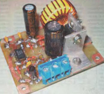
The appearance of the assembled device board is shown in Fig. 2. Transistor VT1 and diode VD1 are installed on heat sinks with an area of 50 cm2. Transistor KP727B (VT1) can be replaced with KP723A-KP723V, KP746A-KP746V, KP812 with any letter index, as well as on IRFZ34N, BUZ11 or other similar devices designed for a direct current of at least 15 A with the lowest possible open channel resistance. Transistor KT201GM (VT2) can be replaced with KT306G, KT312V, KT342A, KT342GM, KT358V, KT375B, KT3102A, KT315B KT315G, KT315E, KT315ZH KT340A, KT340B, KT503B, KT503G, BC547A or other npn transistors with a base current transfer coefficient of at least 100 at collector current 1 mA. Schottky diode KD272A can be replaced by 2D2998B 2D2998V KD2998V- KD2998D, MBR1635, MBR1645 and any of the 2D252, KD272, KD273, 2D2992-2D2997, 2D2999 series, as well as other Schottky diodes designed for a forward current of at least 15 A and a reverse voltage of at least 25 V. The 2S218Zh (VD2) zener diode can be replaced with KS218Zh, KS518A, KS508G, KS509B, 1 N4746 or another with a stabilization voltage of 18 V. For more precise adjustment of the output voltage, selection of a zener diode may be required. Микросхема таймера КР1006ВИ1 (DA1) может быть заменена на КР1441ВИ1, КР1087ВИ2 NE555N Дроссель L1 намотан проводом ПЭВ-2 диаметром 1,25 мм на двух сложенных вместе кольцевых магнитопроводах КП27х15x6 из пермаллоя МП 140. Подойдет и несколько более тонких проводов, соединенных в жгут с общей cross-sectional area about 1 mm2. The winding contains 16 turns. You can also use a yellow-white ring magnetic core T106-26 from Epcos from a multi-winding inductor in the computer power supply. In this case, leave the winding present on the inductor (24 turns of wire with a diameter of 1 mm), the remaining windings are removed. When winding independently, it is made into one full layer of PEV-2 wire with a diameter of 1...1,25 mm. Other chokes with an inductance of at least 18 μH, designed for triple the maximum load current, are also suitable. The inductance of the inductor should not be too high: if it increases above 100 μH, the stabilizer may lose stability. Oxide capacitors C2 and C4 must be designed for a permissible ripple current of at least 3 A and have as low an equivalent series resistance (ESR) as possible, i.e. belong to the “Low ESR” category. This allows you to reduce output voltage ripple and increase the reliability of the device. For example, Jamicon WL series capacitors are suitable. If necessary, each capacitor C2 or C4 can be replaced with several identical capacitors connected in parallel. In this case, we can roughly assume that the permissible ripple current increases in proportion to the number of connected capacitors. Capacitor C3 is installed in close proximity to microcircuit DA1. Capacitors C3 and C5 must be ceramic. The input connections to the on-board network and the output to the laptop are made in the same way as in the prototype. Connecting wires - flexible, copper, multi-core in PVC insulation with a cross-section of at least 2,5 mm2. To connect to the vehicle's on-board network, a cigarette lighter plug with an internal fuse FU1 is used. Please keep in mind that the input current of the device can reach 10 A. It should not flow through the spring inside the cigarette lighter plug. To do this, the spring is duplicated with a wire with a cross-section of at least 1 mm2. The converter is connected to the laptop using the appropriate plug. For example, Acer laptops usually use a cylindrical plug with dimensions of 5,5x1,7x10,7 mm (external, internal diameters and length); for Asus laptops - 5,5x2,5x10,7 mm. The central contact of the plug is connected to the +19 V output. Author: K. Gavrilov
Artificial leather for touch emulation
15.04.2024 Petgugu Global cat litter
15.04.2024 The attractiveness of caring men
14.04.2024
▪ Stream S03 portable hard drives with USB 3.0 interface ▪ New way to remove hydrogen from silicon surface ▪ RS485 transceivers do not require terminating resistors
▪ section of the site Lecture notes, cheat sheets. Selection of articles ▪ article Forty Forty. Popular expression ▪ article What is hard water? Detailed answer ▪ article by Dolichos. Legends, cultivation, methods of application ▪ article Probe for dialing installation. Encyclopedia of radio electronics and electrical engineering ▪ article Cup of tea. Chemical Experience
Home page | Library | Articles | Website map | Site Reviews
www.diagram.com.ua |


 Leave your comment on this article: