|
|


 Arabic
 Bengali
 Chinese
 English
 French
 German
 Hebrew
 Hindi
Hindi Italian
 Japanese
 Korean
 Malay
Malay Polish
 Portuguese
 Spanish
 Turkish
 Ukrainian
 Vietnamese
|
ENCYCLOPEDIA OF RADIO ELECTRONICS AND ELECTRICAL ENGINEERING Car VHF FM tuner. Encyclopedia of radio electronics and electrical engineering
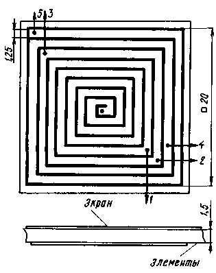
Encyclopedia of radio electronics and electrical engineering / radio reception The creation of specialized microcircuits that provide signal processing in the high-frequency paths of broadcasting receivers has led to the "unification" of their construction. When creating receiving devices, radio amateur designers, in essence, were left with only the sphere of saturating the design with a functional service. Below is a description of the car receiver, in which, in addition to the power switch, there are only three control buttons for switching subbands and tuning to a station operating within the subband. The design provides for automatic scanning when searching for a station, which is very convenient, especially in cases where the driver cannot be distracted from the traffic situation. When developing the described VHF FM tuner, the following tasks were set: - taking into account the features of the operation of electronic equipment in a car; - simple push-button control of operating modes; - availability of automatic search and scanning mode; - the ability to listen to the sound accompaniment of programs of the 1st-5th TV channels; - unipolar supply voltage 12...17V; - high sensitivity; - good repeatability. The tasks set were achieved using typical but rarely used modes of operation of the LSI VHF FM receiver K174XA34, electronic switching of subbands with pin diodes, non-standard inclusion of the KR572PA1 DAC and an additional input high-linear preselector. Main technical characteristics: - sensitivity - not less than 1,5 μV (with a typical sensitivity of receivers with a similar microcircuit 6 μV); - ranges of received frequencies -55.5...66, 65...77, 82...99, 92...110 MHz; - consumed current - no more than 50 mA. The remaining characteristics of the tuner are determined by the parameters of the LSI K174XA34 [1]. The electrical circuit diagram of the receiver is shown in fig. 1. It consists of three main parts: the radio receiving path A1 (input stage on the transistor 1VT1, LSI K174XA34, subband switching device on the multiplexer 1DD1 and pin diodes 1VD1, 1VD2, 1 VD4,1 VD5), control unit A2 (control buttons SB1 -SB3, elements 2DD1.1, 2DD1.4, triggers 2DD2, 2DD3, comparator 20A1, multivibrator on elements 2DD1.2, 2DD1.3, reversible counters 2DD4 - 2DD6, DAC on chips 2DA2, 2DA3) and display unit A3 (keys on transistors 3VT1-3VT5, LEDs 3VD5-3VD8). Electrical circuit diagram of the receiver (80 Kb) The main functions of the control unit are the formation of a signal that controls the tuning frequency of the receiving path, and the switching code of the subbands. The control unit works as follows. When the power is turned on, a pulse is generated at the output of the inverter (element 2DD1.1), which sets the triggers 2DD3.1, 2DD3.2 to the zero state and writes information from the inputs of the preset counters 2DD4 - 2006 to their outputs, as a result of which the initial subrange 65 is selected ...77 MHz, the minimum voltage is set at the output of the DAC (microcircuits 2DA2 and 2DA3) and, accordingly, the lower frequency of the subband in the receiving path. The lower 10 bits of the output code of the counters determine the voltage at the DAC output, and the upper two - one of the four sub-bands, so that when choosing or searching for the necessary radio station, the transition from sub-band to sub-band occurs automatically in a cycle, i.e. pre-selection of the sub-band is not possible. When you press the increase button SB3 ("+") or the decrease button SB2 ("-") of the tuning frequency, the 2DD2.1 RS-trigger generates the corresponding signal to increase or decrease the output code of the reversible counters, and the 2DD3.1 trigger issues a generation enable signal multivibrator on elements 2DD1.2 and 2DD1.3, supplied to pin 2 of element 2DD1.2 through an integrating RC circuit 2R14, 2C6 and an inverter on element 2DD1.4. Fixing the output state of the counters should occur after the appearance and reliable capture of the input radio signal by the PLL system of the tracking demodulator, which is included in the functional blocks of the LSI K174XA34. Such operation of the receiver is provided as follows. The appearance of a radio signal receiver close to the tuning frequency is accompanied by a change in voltage at pin 2 of the LSI 1DA1, the envelope of which is selected by the 2VD1, 2C1, 2R3 circuit and converted by the 2DA1 comparator into a logical unit, supplied through the dividing circuit 2C3, 2R5 to the information input of the trigger 2DD3.1. At its output, this signal appears after the next clock pulse. However, the multivibrator generation will be prohibited with a delay determined by the time constant of the 2R14, 2C6 circuit. In addition, the same circuit will average short-term random operation of the comparator from radio interference. As a result, at the capture stage, the natural frequency of the tunable PLL oscillator is "pulled up" to the frequency of the input signal. When you press the button SB1 "Scanning" ("Scan"), the tuning frequency of the receiver will begin to change depending on the previously set state of the 2DD2.1 RS-trigger. At the same time, a pulse is generated at the output of the one-shot (RS-trigger 2DD2.2), which is applied to the counting input of the trigger 2DD3.2, as a result of which a log appears at its direct output. 1. The processes of capturing the radio signal and setting the center frequency in the PLL system in this case are the same as those described earlier, however, the hold mode is interrupted after 5 s if the "Scan" button is not pressed again, and scanning continues further until the next radio signal appears. Log state duration. 1 in time is 5 s and is determined by the elements 2R12, 2C5. At the input of the receiving path, a preselector is turned on, attenuating signals outside the band 55 ... 110 MHz. It is a combination of high-frequency filters: T-shaped on elements 1 C1,1 L1, 1C2 and L-shaped on elements 1L3,1, 7CXNUMX. A feature of the amplifying stage on transistor 1 VT1 is an increased dynamic range due to the use of an RF low-noise transistor of the KT368AM type and the presence of current and voltage feedback generated by resistors 1 R4 and 1 R1, respectively [2]. Taking into account the attenuation in the filters, the transmission coefficient of the entire preselector, measured from the antenna input to the UHF LSI K174XA34 input (pin 12), smoothly increases from 6,5 dB at a frequency of 55 MHz to 12 dB at a frequency of 110 MHz. This frequency response makes it possible to some extent compensate for the decrease in sensitivity depending on the increase in frequency observed in LSI K174XA34. A feature of the inclusion of LSI K174XA34 is the use of a generator inductor 1L4, switched by pin diodes 1VD1, 1VD2, 1 VD4,1, 5 VD1. Together with them, the capacitors 15C1, 22C1, 24C1, 26C1 for alternating current close the right taps of the inductor according to the scheme to a common wire. In a typical switching circuit, the VCO supply voltage of the microcircuit is supplied through a similar inductor [1], in the considered circuit, the supply voltage of the entire microcircuit is determined by the voltage drop across the quenching resistor 16 R1, the internal resistance of the 1DD174 multiplexer keys and the voltage drop across the pin diode. The amount of current flowing through the latter is sufficient for normal switching ranges and provides the necessary quality factor for stable generation. For the above switching circuit, the supply voltage must be stable and exceed the supply voltage of the BIS K34XA2,7, which is in the range of 3,3 ... XNUMX V. The source follower on the field-effect transistor 1VT2 eliminates the influence of the circuits following it and shifts the level of the constant component present at pin 2 of the K174XA34 LSI. The display unit displays the number of the working subrange by the glow of the corresponding LED. The search mode is accompanied by the flashing of this LED due to the key switching on the 3VT1 transistor of the variable component of one of the output signals of the reversible counter. The design of the tuner can be arbitrary, depending on the conditions of use and the capabilities of the radio amateur himself. The printed circuit board for the entire device has not been developed, special requirements apply only to the 1L4 inductor. It is printed, its configuration is shown in Fig. 2. Lines show cuts made with a cutter with a blade width of 0,25 mm. The points indicate the places where the pin-diode pins and the pin of the 1C21 capacitor connected to point 1 are soldered. Pin 25 of the BIS 5 DA1 is connected to the same point with an MGTF wire no longer than 1 mm. The entire inductor is surrounded by a screen ring.
For the remaining elements of the receiving path, surface mounting was used on the same side of the double-sided board, the second side being the screen. It should be noted that the inductance of the 1L4 coil for research and experimental purposes was chosen with a margin. Frameless inductors 1L1, 1L3 are wound turn to turn with a silver-plated wire with a diameter of 0,8 mm on a mandrel with a diameter of 3,4 mm and contain 9 and 6 turns, respectively. The 1T1 transformer is wound with two PEV-0,28 wires at once on the K5x3x1 ring made of M20VCh-3 ferrite, each of the windings contains 14 turns, the winding is ordinary. In the manufacture of the regulator, resistors of the MLT-0,125 type or the like were used. Resistors 2R6-2R8 can be in the range of 27 ... 68 kOhm. Resistors 1 R1, 1R4, 2R16, 2R19 have a tolerance of ±5%. Trimmer resistors - type SPZ-38 or the like, for the automotive version it is better to use closed resistors of the type SPZ-19. Instead of the KT368AM transistor, the KT399AM is suitable. Chip K561IE14 can be replaced by 564IE14 or K561IE11 (564IE11). In the second case, a log is fed to the input of the initial state setting (pin 9). 0. Capacitors 1C23, 2C1, 2C3 - type K73-14 or K73-17; 2C5 - type K53-4 with a tolerance of at least ± 20%; 1C25,1C3O - type K50-35; the rest - ceramic, of any type; capacitors 1C1, 1C2, 1C7 must have a tolerance of ± 5% and TKE M75, blocking can be groups TKE H90, the rest - normalized TKE no worse than M750. High-frequency inductor 1L2 - type DM-1,2 with the inductance value indicated on the diagram. After checking the operating modes of the tuner elements and the performance of the blocks that do not require adjustment, the receiver tuning is as follows. 1. Using a trimmer resistor 2R17 for the 1VD3 varicap, set the initial bias voltage of 2,2 V at the output of the DAC (pin 6 of the op-amp 2DA3) in the initial state of the reversible counter 2DD4 -2DD6, at the output of which, after applying the supply voltage, code 0111 1111 1111 (high level - junior category). Then, increasing the generation frequency of the multivibrator by decreasing the capacitance of the 2C7 capacitor, use an oscilloscope to verify the linearity of the change in the output voltage of the entire DAC. With voltage restrictions, you should select the values \u2b\u16bof the resistors 2R19, XNUMXRXNUMX. 2. Using the 2R2 trimming resistor, set the 2DA1 comparator threshold to ensure reliable capture and retention of the radio signal. To do this, apply a test FM signal to the receiver input with a level corresponding to the nominal sensitivity, use the SB2 or SB3 buttons to turn on the search mode. If necessary, reset to the initial state - by turning off the supply voltage of the control unit. Another way is to receive obviously the weakest radio signal. 3. Specify the pin-diode pin connection positions on the 1L4 printed inductor in accordance with the specified technical specifications. To do this, apply a log to the information input of the trigger 2DD3.1. 1, the generation prohibition is disabled. Then, from the reference oscillator, apply an FM signal with the frequencies of the lower boundaries of the subbands to the receiver input from the reference generator, set zeros on the control inputs of the DAC 2DA3 using the SB2 or SB3 buttons, and set the code of the corresponding subband on the control inputs of the multiplexer 1 DD1. Between pins 10 of the 2DD3.1 chip and common wires, a resistor with a resistance of about 10 MΩ is required. Literature
Author: Yu. Ezhkov, Omsk; Publication: N. Bolshakov, rf.atnn.ru
Energy from space for Starship
08.05.2024 New method for creating powerful batteries
08.05.2024 Alcohol content of warm beer
07.05.2024
▪ A new way to control smart watches ▪ Wind farms could work on Mars ▪ Breaking the record for the length of a quantum communication line ▪ Updated EU requirements for power consumption of appliances in sleep mode
▪ section of the site for the Builder, home craftsman. Selection of articles ▪ article The state is me. Popular expression ▪ article When did you first use combs? Detailed answer ▪ article Serpukha bract. Legends, cultivation, methods of application ▪ vegetable cutter article. Focus Secret
Home page | Library | Articles | Website map | Site Reviews
www.diagram.com.ua |

 Leave your comment on this article: