|
|


 Arabic
 Bengali
 Chinese
 English
 French
 German
 Hebrew
 Hindi
Hindi Italian
 Japanese
 Korean
 Malay
Malay Polish
 Portuguese
 Spanish
 Turkish
 Ukrainian
 Vietnamese
|
ENCYCLOPEDIA OF RADIO ELECTRONICS AND ELECTRICAL ENGINEERING Car radio station in the range of 144 ... 146 MHz. Encyclopedia of radio electronics and electrical engineering
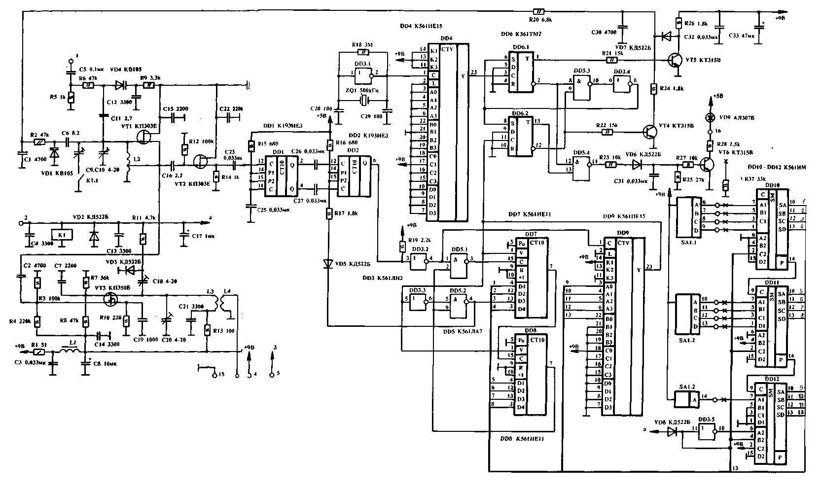
Encyclopedia of radio electronics and electrical engineering / Civil radio communications Schematic diagram of the frequency synthesizer is shown in Fig.1. It is based on a phase locked loop (PLL) ring and a frequency divider with a variable division ratio (CVD). The controlled oscillator operates at frequencies of 133,3 - 135,3 MHz when receiving and at frequencies of 144 - 146 MHz when transmitting. It is made on a transistor VT1 type KP303E according to the inductive three-point scheme. Its frequency is tuned using a varicap VD1 type KB 105 voltage coming from a pulsed phase-frequency detector (IPFD) through a low-pass filter made on the elements C30, R20, C1. The frequency shift during the transition from reception to transmission by 10,7 MHz is carried out by connecting capacitor C9 using relay contacts K1.1. Although this is not the best way, it is quite simple in terms of circuitry and has proven itself well in work. From the voltage-controlled generator, the signal is fed to a buffer amplifier based on a VT3 transistor of the KP350A type. The amplified signal is allocated on the L3.C18.C20 circuit and is fed through the L4 communication coil to the receiver and transmitter boards. The restructuring of the circuit during the transition from reception to transmission is carried out by applying voltage to the VD3 diode and connecting the capacitor C 18 to the common wire. The signal arriving at the DPCD is also buffered by an emitter follower on a VT2 transistor of the KP303E type. The modeling voltage is applied to terminals 1 of the synthesizer board and fed to the VD4 varicap of the KB105 type. Frequency modulation with small deviation is carried out by changing its capacitance. The frequency deviation is 3 kHz. The synthesizer reference frequency generator is made on the DD3.1 element and operates at a frequency of 500 kHz. You can use another quartz resonator for frequencies up to 3 MHz, but it is necessary to reset the division factor of the divider with a fixed division factor, made on a D4 chip of the K561IE15 type, so that a frequency of 12,5 kHz is present at its output. The division factor is set by the appropriate wiring of the installation inputs of the microcircuit. DPKD is built on elements D1 - D9. The high-frequency prescaler by 10 is made on a D4 chip of the K193IEZ type. Its output 12 receives voltage from the emitter follower VT2. The high-frequency 10/11 prescaler is made on a D2 chip of the K193IEZ type. The absorbing counter is built on D7, D8 microcircuits of the K561IE11 type, a low-frequency divider with a variable division ratio is based on the D9 microcircuit of the K561IE15 type. The frequency of the input signal is reduced by a factor of 1 with D10. Then the signal goes to the divider D2, which, depending on the control signal at pins 14, 15, operates in the mode of dividing by 10 or 11. The DPKD division coefficient is determined as: N=A+100*B, where O<A<99, 1<B <A. A, B - coefficients set by the frequency setting node. So, let's say, during transmission, the frequency is set to 144250 kHz, then: 144250 kHz: 12,5 kHz = 11540, then 11540: 100 = 115,40 V = 115;. A = 40, and so on at other set frequencies. When transmitting, the division factor will vary within 11520 - 11680, while receiving - 10664 -10824. From the output D2, the pulse sequence is fed through the blocking circuit D5 to the counting input of the programmable counter D9. Upon reaching the zero state of the counter D9 is formed at its output pulse of positive polarity with a duration equal to the period of the input signal. With the help of counters D7, D8, the divider D2 is controlled. These counters generate a control action of positive polarity with a duration varying from 0 to 99 periods of the signal received at the counting input, depending on the code set on the information inputs D7,08. Let us explain the work of the DPKD in general. We will assume that D7, D8 are in the zero state with a logical zero at the output, and an output pulse is formed at the output of D9. When a signal appears at the output D9, the code set at the information inputs D7, D8 is recorded, as well as the division coefficient code D9 is recorded. This operation is performed by transferring D9 from the zero state to the state corresponding to the set DPKD code. At the same time, a "log.8" signal appears at the output of D1, which, through D5.2, switches D2 to the mode of division by 11, and also allows the passage of output pulses from D2 through D5.1 to the counting input D7. At the end of the counting cycle, a "log.8" signal appears at the output of D0, which blocks the receipt of clock pulses at its counting input and switches D21 to the division mode by 10. When the zero state of D9 is reached, the next pulse is generated at its output, which determines the end of the previous cycle account and start a new one. Then the whole cycle is repeated.
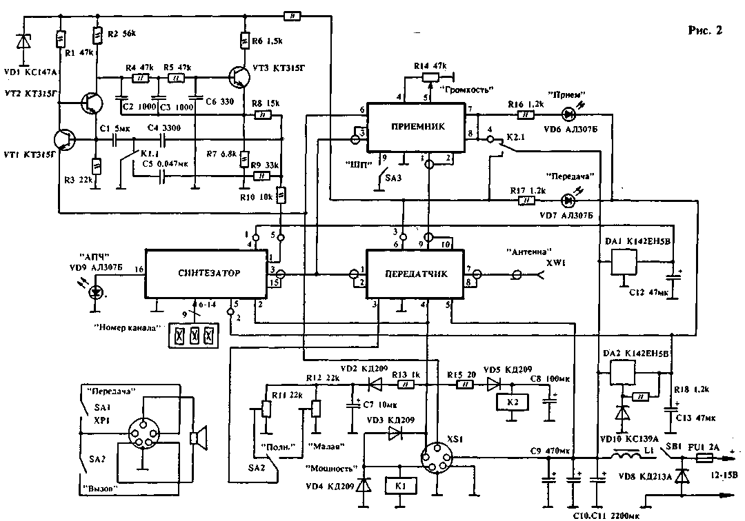
The pulse frequency-phase detector with a synchronism control indicator is built on the elements D3, D5, D6 and transistors VT4, VT5. One of the inputs of the ICFD receives a signal from the reference oscillator, and the other from the DPKD. The comparison is carried out at a frequency of 12,5 kHz. The digital part of the discriminator is made on D-flip-flops D6.1. In this case, most of the time, with a small phase difference of the input signals, there is a low potential on the collector of the transistor VT1 and the VD7 diode is locked. With a zero signal at the direct output of D6.1, the charge current feeds the input of the low-pass filter C30, R20, C1. The discharge current generator on the transistor VT4 is controlled from the inverse output D6.2. The synchronism control indication unit is built on the D5.4 element and the VT6 transistor. If there is synchronism, the VD9 LED will be extinguished. The frequency setting unit is made on the SA1 switch of the PP8-3 type or any other, operating in binary-decimal code and adders D10 - D12 of the K561IM1 type. The second inputs of the adders are set to 520 when transmitting and 664 when receiving. The switching of numbers is carried out by applying a control signal to the D12 chip through the VD8 diode and the D3.5 element. Ordinary position switches can also be used as a frequency setting switch, supplementing the frequency setting unit with an encoder made on ROM or diodes. The synthesizer is powered by two power supplies 5 V and 9 V. The 5 V power supply is used to power the D1 and D2 microcircuits. All other microcircuits are powered by a 9V power supply. Frequency number switch SA1 and LED VD9 are installed on the front panel of the radio station; The connection diagrams of the common board and headset are shown in Fig.2. The headset includes a dynamic head type 0.25GDSh2 or any other and two microswitches of the MT-3 type and is connected to the radio station using a twisted cord and an XP1 plug. The SA1 button of the headset is used to switch to the "Transmission" mode. When the SA2 headset button is pressed, the radio enters transmit mode and dial tone is activated. In receive mode, the signal from the antenna through the WA1 connector goes to the transmitter board, where the antenna relay is located, and then through its contacts to the receiver board (pin 1 of the board). The signal from the frequency synthesizer is also fed here through pin 3 of the board. The low-frequency signal from pin 6 of the receiver board goes through socket XS1 to the dynamic head of the headset.
In transmission mode, the signal from the dynamic head of the headset, through the XS1 jack, goes to the microphone amplifier on transistors VT1 and VT2 of the KT315G type and through a low-pass filter with a cutoff frequency of 2,5 kHz on the VT3 transistor goes to the synthesizer modulator. When you press the "Call" button on the headset, relay K1 is activated and closes contacts K 1.1, which puts the microphone amplifier into the mode of generating a sinusoidal signal with a frequency of about 1,5 kHz, which also goes to the modulator. Pressing this button also puts the radio into transmission mode. Switching the radio station from reception to transmission is carried out by pressing the PTT of the headset "Transmission". In this case, relay K2 is activated, which switches the supply voltages to the radio station nodes corresponding to the transmission mode. The operation of the relay K2 is delayed by several tens of milliseconds using the chain R15, C8 with respect to switching the synthesizer to the transmission mode, to which the voltage is applied directly. This is necessary in order to prevent the radiation of power from the antenna at the time of tuning the synthesizer. A frequency-modulated signal with a deviation of about 3 kHz enters the transmitter board through pins 1, 2 of the board, is amplified and enters the antenna through the XW1 connector. In this case, the antenna relay on the transmitter board is switched to transmit mode. Switch SA2 is used to switch the power of the transmitter. In the "Full" position the full power is emitted about 15 W, and in the "Low" power position - about 1 W. Resistors R11 and R12 are used to set the power. The R13, VD2, C7 chain allows, when the radio station is switched to transmission mode, to obtain a smooth increase in transmitter power for several milliseconds. This is necessary to improve the reliability of its operation. If desired, you can install an SWR meter in the feeder at the output of the transmitter and start its output to pin 3 of the transmitter board, which will automatically reduce its power in case of antenna mismatch and significantly increase the reliability of the output stage. Switch SA3 is used to turn off the noise reduction system. Resistor R 14 - volume control, LEDs VD6 and VD7 indicate the transition from receive to transmit mode, LED VD9 indicates the PLL capture of the synthesizer. The supply voltage filter that prevents interference from the vehicle's on-board network from the ignition system to the radio station is made on the inductance L1 and capacitors C9 - C 11. The VD8 diode protects the radio station from entanglement of the supply voltage. If it is present, the fuse FU1 will fail. Voltage stabilizers are made on DA1 and DA2 microcircuits. The chain R18, VD10 serves to raise the stabilization voltage of the DA2 chip to 9V. Author: V. Stasenko; Publication: N. Bolshakov, rf.atnn.ru
A New Way to Control and Manipulate Optical Signals
05.05.2024 Primium Seneca keyboard
05.05.2024 The world's tallest astronomical observatory opened
04.05.2024
▪ Scientists have perfected the web ▪ Nokia CDMA phone with GPS module ▪ 28nm Embedded Flash for Microcontrollers
▪ section of the site Stories from the life of radio amateurs. Selection of articles ▪ article Piano in the bushes. Popular expression ▪ article What is quartz? Detailed answer ▪ article Ginseng real. Legends, cultivation, methods of application ▪ article Magnetically hard materials. Encyclopedia of radio electronics and electrical engineering ▪ article Nogai proverbs and sayings. Large selection
Home page | Library | Articles | Website map | Site Reviews
www.diagram.com.ua |

 Leave your comment on this article: