|
|


 Arabic
 Bengali
 Chinese
 English
 French
 German
 Hebrew
 Hindi
Hindi Italian
 Japanese
 Korean
 Malay
Malay Polish
 Portuguese
 Spanish
 Turkish
 Ukrainian
 Vietnamese
|
ENCYCLOPEDIA OF RADIO ELECTRONICS AND ELECTRICAL ENGINEERING Stabilization of class AB amplifiers. Encyclopedia of radio electronics and electrical engineering
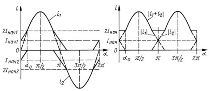
Encyclopedia of radio electronics and electrical engineering / Transistor power amplifiers The article presented to the attention of readers presents a method for automatically adjusting the bias voltage of push-pull amplifiers to stabilize the current consumed by the amplifier when the amplified signal passes through zero and at rest. The advantages of the article include the methodology for calculating and checking the stability of the UMZCH output stage mode. Class AB amplifiers are the most common among linear power amplifiers, since they allow you to combine the high efficiency of class B amplifiers with the absence of distortion in class A amplifiers. However, the formation of the transistor bias voltage necessary for this, supporting the arms of the push-pull cascade in the optimal initial current (quiescent current) mode, was and remains the main problem of constructing such amplifiers, the problem of stabilizing their parameters. This is explained by the instability of the characteristics of transistors, their dependence on temperature and signal level, as well as on the spread and drift of the parameters of the same transistors. Article [1] deals not so much with stabilization as with ensuring the "certainty" of the regime. The achieved practical level is characterized by a selection of schemes in [2]. From them and from other publications known to the author, it can be seen that there is still no acceptable circuit solution for stabilizing the mode of amplifiers of this class; no unambiguous method (rule, criterion, algorithm) for regulating the bias voltage has been formulated, which would allow automatically setting the optimal bias voltage for powerful transistors. One solution to this problem is suggested below. Optimality criterion The amplifier mode is most effectively stabilized by feedback methods by measuring a certain electrical quantity that depends on the bias voltage, comparing it with a reference value, and automatically regulating it. Attempts to stabilize the quiescent current of amplifiers by adjusting the bias voltage led either to only a partial solution of the problem [3, 4], or to the creation of amplifiers [5] that have the necessary stability, but lose to high-quality class AB amplifiers in some parameters. The current of these amplifiers at the moment the amplified signal passes through zero - it is called the initial current - is not equal to the quiescent current of the amplifiers; they are more correctly classified as dynamically biased amplifiers. For push-pull amplifiers with stabilization of the minimum currents of the arms [6], in addition, overexcitation is dangerous. Only class AB amplifiers that are stable in all respects can be considered perfect, out of competition. The criterion for the optimal bias voltage of class AB amplifiers is the stability of the initial current, equal to the quiescent current of the class AB amplifier and maintained automatically. This optimality criterion without its formulation and without separation of the concepts of quiescent current and initial current was used in [7]. However, the author chose an unsuccessful method for determining the initial current (in the author's terminology - the quiescent current) by calculating it using operational amplifiers as the difference between the measured currents of the shoulders and the load. In addition to the complexity of implementation and rather large power losses in the measuring resistors, the main disadvantage of the chosen technique is that the determination error may exceed the desired value. The development of ideas from [7] can be considered a technical solution [8], where a good result is achieved in relation to field-effect transistor amplifiers, but the requirements that are mandatory for any class AB amplifiers are not fully formulated and fulfilled. Below, we consider in detail the method for measuring the initial current using a detector of the minimum values of the sum of currents in the arms of a push-pull cascade. Theoretical justification In order to identify the possibility of measuring the initial current in a push-pull cascade against the background of changing signals, we consider the changes in currents in the arms of such a cascade and their sums, assuming that the signal current in the load changes according to the simplest sinusoidal law: iн = lmsinα. Here iн - instantaneous value of the load current; Im - its amplitude; α = Ωt - phase angle; Ω - operating frequency; t - time. The nature of the change in currents in the shoulders of a push-pull cascade is shown in Fig. 1,a, and the sums of the absolute values of the currents - in fig. 1b.
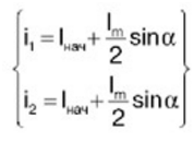
The load current in a push-pull stage is determined by the difference in the currents of the shoulders or the sum of the absolute values of the increments of the currents of the shoulders iн = |Δi1| +lΔi2|. At low signal currents, both arms of the amplifier operate in a class A linear mode. The increments of the currents of the arms are equal in absolute value to half the load current: |Δi1| +lΔi2| = 0,5iн = 0,5lmsinα, and the expressions for the shoulder currents will have the form
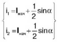
for 0 ≤ α ≤ α0. Here and below, through α0 the phase angle is indicated, above which the amplifier switches from the class A mode to the mode with current cutoff in the arm. If all currents are normalized with respect to the maximum load current (normalized currents are indicated in bold) IBeg/Im = IBeg и Im/Im = 1 then for 0 ≤ α ≤ α0. For α = α0 the current of the second arm decreases to zero, i.e. iBeg - 0,5sinα0 = 0. From this we determine α0 = arcsin2ISTART. In the current cutoff mode in one arm, the load current is determined by the increments of the current of the other arm:
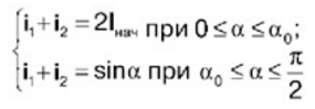
for α0 ≤ α ≤ π/2. For α ≥ π/2, the nature of the change in currents is repeated in the reverse order, and for α > π, the sign of the load current changes and its formation is carried out by another arm (see Fig. 1). Sum of shoulder currents
has a constant minimum value, determined only by the initial current of the amplifier (i1 + i2)min = 2IBeg. This makes it possible to formulate a stabilization method: to stabilize the class AB amplifier mode at any desired initial current, it is necessary and sufficient to stabilize the minimum value of the sum of the currents of the arms, which is equal to the double value of the initial current of one arm. Generalized block diagram On fig. 2 shows the simplest amplifier circuit with initial current stabilization according to the proposed method. It was obtained by modifying the circuit from [4] by including a resistor R13 and a peak detector on a VT8 transistor. The voltage pulses across the resistor R13 are maximum at the minimum total voltage across the resistors R10 and R11, i.e., in the rest mode of the amplifier and when the signal passes through zero. The emitter current of the transistor VT8 charges the capacitor C3 to a voltage just below the maximum voltage across the resistor R13. In this case, the voltage at the input of the bias voltage regulator VT3 is the greater, the lower the total voltage across the resistors R10 and R11. With a decrease in the initial current of transistors VT6 and VT7, the bias voltage increases, and as they increase, it decreases. As a result, the initial current of the terminal stage transistors stabilizes at the level of the quiescent current.
Regardless of the specific design, whether it is a transformer or transformerless amplifier with parallel or series connection of the arms, it is possible to name the elements that are mandatory for stabilizing its mode. These elements are shown in Fig. 3, some of which are used, in particular, in the amplifier, the circuit of which is shown in fig. 2. The generalized circuit includes the amplifier itself and the bias voltage regulator, with the exception of the load R„. The bias voltage regulator is transistor VT3 with resistor R6.
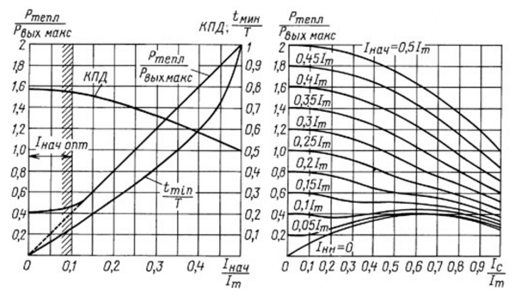
Current sensors 1 and 2 in two arms of the amplifier in fig. 2 are resistors R10 and R11; the summing device is implemented by connecting these resistors in series: a voltage proportional to the sum of currents is removed from them. Using the transistor VT3, the minimum total voltage is inverted into the maximum voltage across the resistor R13. The detection of this voltage is carried out by a transistor VT8 with an RC circuit R12C3. It is expedient to combine all these elements into a special stabilization module, since it is they that together stabilize any given initial amplifier current and ensure that this current is equal to the quiescent current. These elements do not participate in signal amplification. Below is a description of a more complex stabilization module designed for a symmetrical amplifier circuit with current sensors located in the power circuits. Selection of initial current Providing the possibility of stabilizing the initial current, it is necessary to justify the choice of its optimal value and the allowable range of change. To select the optimal current IBeg consider the dependence of the main parameters of a class AB amplifier on the initial current, which varies within the maximum limits, i.e. from zero (class B) to 0,5Im (class A) and on the amplitude of the signal current. The calculated graphs of the dependence of these parameters on the initial current of the amplifier are shown in Fig. 4a.
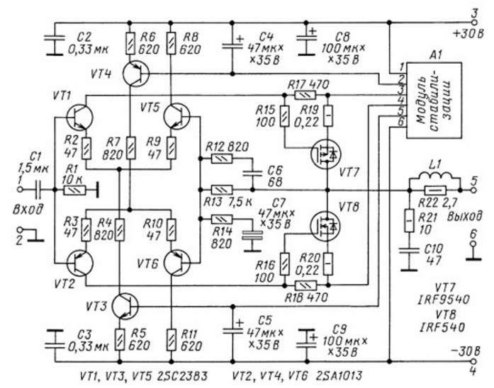
The efficiency curve characterizes the dependence of the maximum efficiency of the amplifier on the selected value of the initial current. With its increase, the maximum efficiency decreases from the value of 0,785, characteristic of class B amplifiers, to 0,5, characteristic of class A amplifiers. Curve Pwarm/Pout max It characterizes the maximum thermal power dissipated in the output transistors from the selected initial current of the amplifier. At the initial current IBeg ≥ 0,13Im, the maximum thermal power is determined precisely by this current at rest of the amplifier (ascending straight section of the curve). With a lower initial current, the maximum thermal power is determined mainly by the power from the alternating signal current, released on the amplifying transistors. For class B amplifiers (at IBeg = 0) the maximum thermal power reaches 0,405Rout max. Curve tmin/T characterizes the relative duration (in fractions of a period) of the minimum of the sum of shoulder currents depending on the initial current: tmin/T = α0/(π/2) = 2α0/C = (2arcsin (2IBeg))/π. This dependence characterizes the required speed (readout time) of the minimum value detector. The duration of the minimum of the sum of currents is the longer, and the requirements for the peak detector are correspondingly lower, the greater the initial current. In class A, a peak detector is not needed at all. As the initial current decreases, the requirements for the peak detector naturally increase. On fig. 4b shows the dependence of the thermal power released on the amplifying transistors on the signal current at different initial amplifier currents. These curves clearly show the zone of optimal values of the initial current. It can be considered a current from 0 to 0,1Im. At the maximum current of this range, there are guaranteed no step-type distortions, and the thermal power released by the transistors in the quiescent mode does not exceed the power allocated to them in the strong signal mode. In the entire possible range of signal currents, it fluctuates around the value 0,4Pout max and maximally exceeds the maximum thermal power of class B amplifiers by only 10%, remaining less than the maximum thermal power of class A amplifiers by 4,5 times. The maximum efficiency of an amplifier with this initial current is 77%, which is only 2% lower than in class B amplifiers. A further increase in the initial current, although acceptable, does not provide any energy gain and almost no reduction in distortion. Reducing the initial current is desirable from the point of view of reducing thermal power losses in the rest mode. Whether this is appropriate is up to the developer. Direct stabilization of the initial current eliminates the danger of working with bias voltages that completely close the amplifier, and thereby the risk of breaking the common negative feedback (CNF) circuit. Non-linear distortion is reduced by means of feedback and can be controlled when setting up the amplifier. In this case, the initial current of the amplifier can be set significantly less than 0,1Im. The upper part of the dynamic range of amplified signals that bring the output stage from class A mode to class AB mode is related by the relation Im/(2IBeg) At an initial current of 0,1Im it is 14 dB, and with an initial current of 0,05Im - 20 dB. If we look at the amplified signal with an oscilloscope, we will see peak values that are 14 ... 20 dB higher than the root-mean-square level of audio signals. This means that if the maximum output power of the amplifiers is used to reproduce precisely these peaks without distorting, then most of the time the amplifier operates at relatively low signal levels, i.e. in class A mode. This justifies the reduction of the quiescent current and, accordingly, the power consumption in this mode. The maximum value of the initial current of the recommended interval is highlighted in fig. 4, but hatched. Experimental Amplifier On fig. Figure 5 shows a diagram of a high-quality medium-power amplifier, which can be loaded with an S-30 speaker system.
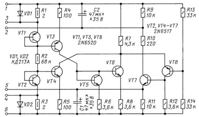
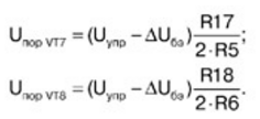
When considering the circuit, conclusions 1 and 3, as well as 4 and 6 of the stabilization module, can be considered closed in pairs. Pins 2 and 5 are anti-phase outputs for controlling bias voltage regulators. The features of the amplifier itself are the use of powerful field-effect transistors in the output stage and the symmetry of the structure for both polarities of the amplified signal. The bias voltage for field-effect transistors is formed on resistors R17 and R18 by the currents of transistors VT1 and VT2, and their automatic adjustment is by synchronous adjustment of the currents of the preliminary stages of the amplifier by transistors VT3 and VT4. Resistors Rl9 and R20 serve to increase the dynamic stability of transistors, elements C10, R21, R22 and L1 - to correct the frequency response of a system with a complex nature of the load. Stabilization module The stabilization module for a symmetrical amplifier circuit has shoulder current meters isolated from the load, and a common power supply is used as a reference voltage source; in addition, the module has two anti-phase outputs. Its scheme is shown in Fig. 6.
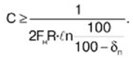
The measuring sensors of the minimum current in the arms of the output stage are resistors R1 and R3, shunted, as in the circuit in Fig. 2, silicon diodes VD1 and VD2 to bypass the high load current. For summation, reduced copies of these currents are used, formed by transistors VT3 and VT4 with current-setting resistors R4 and R5. Transistors VT1 and VT2 are used to compensate for the base-emitter voltage of transistors VT3 and VT4. Due to this, the voltage across the resistors R4 and R5 can be considered equal to the voltage across the resistors R1 and R3, and the current transfer coefficient from the meters to the copy stages is equal to the ratio of the resistances of the resistors R1 to R4 and R3 to R5. The summing device is implemented on the resistor R7. A scaled copy of the current of the lower arm of the output stage is supplied to it directly through the VT4 collector, and a copy of the upper arm current corresponding to the same scale is fed by the transistor VT3 through the current mirror on transistors VT5, VT6 with resistors R6 and R8. The currents of transistors VT4 and VT6 are added to the current of the transistor VT8 across the resistor R7. At the same time, the minimum sum of the currents VT4 and VT6 turns into a maximum current VT8, i.e., the maximum voltage across the resistor R12 when the amplified signal passes through zero and in the rest mode of the amplifier. At rest, this voltage is constant and maximum. As the signal amplitude grows, it first gets small and rare, then deep and long dips, acquiring the form of a chaotic curve, vertices tied to the maximum voltage values. The deepest dips correspond to the largest signal amplitude, the longest dips correspond to the lowest amplified frequencies; flat tops correspond to the operation of the amplifier in class A mode, the centers of the tops correspond to the moments when the amplified signal passes through zero. The peak detector on the transistor VT7 quickly charges the capacitor C1 to a voltage slightly lower (by ΔUba ≈ 0,6 V) maximum voltage across the resistor R12. Time constant τzar ≈ C1 R12/h21E7, where h21E7 - current transfer coefficient of the base of the transistor VT7. Discharging is slower. Its time constant τtime ≈ C1 R11. Ratio τzar/τtime = R12/(R11 h21E7) should be no more than the relative duration of the minimum sum of the currents of the arms, since charging (reading information about the minimum sum of currents) should be as fast as possible, and discharging (storing this information until the next reading) should be as long as possible: τzar/τtime ≤ tmin/ T. The heaviest mode of operation of the peak detector is the maximum signal mode at the lower amplified frequency Fн when the voltage dips across the resistor R12 are maximum both in depth and duration. According to the permissible amplitude of ripples on the capacitor C1 in this mode δп, expressed as a percentage, with a known discharge resistance (R11 in the circuit of Fig. 6), you can also calculate the minimum capacitance of this capacitor
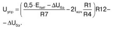
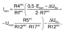
The voltage across this capacitor is constant when the amplifier is at rest. In the amplification mode, this voltage acquires shallow (measured by units or fractions of a percent) sawtooth pulses at the place of input voltage dips when the amplifier exits class A mode, with a slow decay and a quick return to the maximum value in class A mode. This voltage, on average, remains proportional to the initial amplifier current and serves as the control voltage of the bias regulators. Control voltage ripple inevitably introduces small distortions at lower signal frequencies. But these distortions are the smaller, the larger the capacitance of the storage capacitor of the detector; they are introduced only in a strong signal that takes the amplifier out of class A, and in a symmetrical circuit, like ours, they are mutually compensated by the amplifier shoulders. In the experimental amplifier, these distortions are not felt in any way. The C7R2 circuit is included in the collector circuit of the VT9 transistor, exactly the same as in the emitter circuit - C1R11. This allows you to get a second anti-phase output of the stabilization module. Resistor R10 serves to limit the inrush current of the transistor VT7 during transients. Setting the initial current of the amplifier is possible by choosing equal resistors R1 and R3, as well as by selecting resistor R7 or R12. The mode of stabilization of this current does not require any subsequent adjustment. Example of calculation of stabilization elements The selected speaker system is designed for an output power of up to 30 watts. With its nominal electrical resistance of 4 ohms and the output power of the amplifier of 15 W, the current amplitude will be 2,74 A. The maximum recommended value of the initial current, equal to the quiescent current of the output transistors, is Iinitial max = 0,1Im = 0,274A. Choose IBeg = 0,1 A. Normalized value IBeg = IBeg/Im = 0,1/2,74 = 0,0365 Since the calculation is subject to a closed-loop system with feedback, all elements of which depend on each other, let's mentally break it at the junction point of the amplifier itself and the stabilization module. Let us set the rated voltage for controlling the bias regulators convenient for operation, which should be set at this point in a linear mode with the selected initial current (quiescent current) Ucontrol = 10 V. This makes it possible to calculate the elements of the two circuits independently of each other. In the amplifier itself (see Fig. 5) for the selected field-effect transistors, the measured threshold voltage is 3,5 ... 3,8 V. With the resistors R17 and R18 indicated in the diagram, this voltage is achieved at a current of transistors VT1 and VT2 in the range 7,45 .8,01...5 mA. Approximately the same currents should have transistors VT6 and VT3. The currents of transistors VT4 and VT1 are equal to the sum of the currents VT3 and VT2 or VT4 and VT15; let's take them equal to 5 mA. In this case, the resistance of the resistors R6 = RXNUMX = (Ucontrol - ΔUba) / IVT3 = (10 - 0,6)/15 10-3 ≈ 620 Ohm. The inequality of the threshold voltage of transistors VT7 and VT8 and the corresponding currents of transistors VT1 and VT2 is achieved automatically by the action of the OOS through the resistor R13, which ensures the equality of the drain currents of transistors VT7 and VT8. We proceed to the calculation of the elements of the stabilization module (see Fig. 6). We choose the resistance of resistors R1 and R3 so that the operating voltage on them, due to twice the initial current, was obviously less than the opening voltage (0,6 V) of the powerful silicon diodes VD1 and VD2: R1 = R3 < Uot/(2IBeg) \u0,6d 2 / (0,1 3) \uXNUMXd XNUMX ohms. Choose R1 = R3 = 2 ohms. The operating voltage across these resistors at rest of the amplifier, controlled when setting it up (more correctly, there is nothing to set up when checking), will be UR1 = UR3 = IBegR1 = 0,2 V. With the selected values R4 = R5 = 100 Ohm, the currents of the transistors VT3 and VT4 will be 50 times reduced copies of the currents of the amplifier arms. In silent mode and when the signal passes through zero, they will be equal to 2 mA. The maximum value of these currents, equal to 7 mA, is determined by the maximum voltage (0,7 V) on the diodes VD1 and VD2. We select the resistance of the resistor R7 from the condition that the maximum current of one of transistors VT3 or VT4 when a sufficiently strong signal passes through the cascade on transistor VT8 can close: R7 = EPete/(2 Imax) \u60d 2 / (7 4,3) \u3d 4 kOhm. It is not dangerous if the maximum currents if the maximum currents of transistors VT7 and VT8 will be slightly more or less than 8 mA. They do not carry information about the initial current of the amplifier, and the VTXNUMX transistor is either closed or its current is minimal. In silent mode or when the signal voltage passes through zero, the VTXNUMX transistor is open and its collector is current maximum: IVT8 max = (0,5 EPete - ΔUba)/R7 - 2IBeg/ 50 \u0,5d (60 0,6 - 4,3) / 2 - (100 50) / 3 \uXNUMXd XNUMX mA. With this current, the nominal control voltage of the bias voltage regulators is formed. The resistance of the resistor R12 is determined from the condition that the constant voltage on it in silent mode or pulsating at the moment the amplified signal passes through zero will be ΔUba greater than the control voltage: R12 = (Ucontrol + ΔUba) / IVT8 max \u10d (0,6 + 3) / 3,6 \uXNUMXd XNUMX kOhm Numerical calculation of the minimum capacitance of the capacitor C1 according to the formula given in the previous section, at Fн = 20 Hz and δп = 3% gives 82 uF. The applied capacitors C1 and C2 have a lower capacitance, but it is doubled by the capacitors C4 and C5 of the amplifier itself (Fig. 5). Checking the performance of the peak detector: τzar/τtime = R12/(R11 h21E7) = 3600/(10000 100) = 0,0036; tmin/T \u2d (2 arcsin (0,0365 0,0465)) / π \uXNUMXd XNUMX. The ratio τzar/τtime ≤ tmin/T is reserved. Let us derive a formula for checking the calculation of the initial current according to the selected and given parameters of the circuit elements. The quiescent current (aka initial) of powerful transistors is determined by their bias voltage, which, with a high or very high steepness of the ascending sections of the characteristics of field-effect transistors, does not differ much from the threshold voltage of these transistors, so we will assume that for any initial current, the bias voltage is approximately equal to the threshold. Given that the currents of the transistors VT3 and VT4 (in Fig. 5) are divided by the transistors of the differential stages in half, we have
The second equality is equivalent to the first, since R5 = R6 and R17 = R18. According to the diagram in Fig. 6 can write
Solving these expressions together, we obtain for the amplifier as a whole
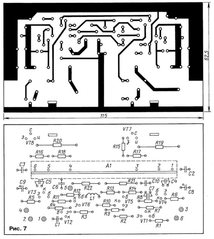
Here, additional indices are introduced to designate the node to which this or that resistor belongs: ms - stabilization module, ms - the amplifier itself. Numerical calculation with substitution into the formula of amplifier data at Upores = 3,5 V gives the value of IBeg = 102,5 mA with an acceptable error. But it is especially valuable to use this formula to evaluate the effect on the initial current of the drift amplifier of certain parameters of the amplifier elements and, first of all, the threshold voltage of field-effect transistors. A completely unacceptable change in U for many amplifierspores transistors by ±20% would lead to their failure or to severe signal distortion. In our case, it only changes the initial amplifier current by ±12,5%, which is quite acceptable and most likely will not even be noticed by listeners. Construction and details The amplifier is made on the basis of the design "Radio engineering U-101-stereo". Two printed circuit boards of the amplifier, corresponding to the drawing in fig. 7, instead of the printed circuit boards of the ULF-50-8 modules, they are installed on the heat sinks of the base amplifier. Terminal transistors VT7 and VT8 are fixed on insulated heat sinks without additional insulation. Amplifier oxide capacitors - K50-35, C7 - non-polar Jamicon NK, the rest - K10-17. Resistors R19 and R20 - C5-16MV, the rest - C2-33H. The L1 frameless choke from the ULF-50-8 module contains 16 turns of PEV-11,3 wire, wound in two layers with an inner diameter of 5 mm.
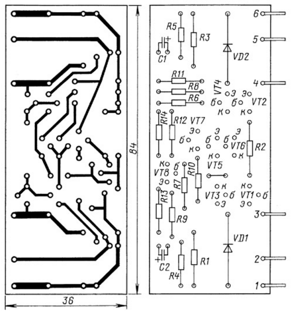
Boards of stabilization modules, the drawing of which is shown in fig. 8, installed perpendicular to the amplifier boards; they are fastened by their conclusions 1-6. Capacitors - K50-35, resistors - S2-33N.
Conclusion The apparent complexity of the stabilization module at first is justified by the effectiveness of the proposed stabilization method, ease of calculation and low power consumption of this module, as well as the almost no need to build an amplifier. This is also confirmed by the flawless operation of the experimental amplifier for several years. Such stabilization of the regime of powerful cascades can be applied both in high-class amplifiers and increased reliability, and in most transistor amplifiers, in control, measurement and automation devices. Literature
Author: V. Efremov
Machine for thinning flowers in gardens
02.05.2024 Advanced Infrared Microscope
02.05.2024 Air trap for insects
01.05.2024
▪ New family of laser diode drivers ▪ Sound stream localization creates the perfect signal ▪ Nanoparticles control immunity ▪ SSDs have no future, scientists say
▪ site section Low frequency amplifiers. Article selection ▪ article My hut on the edge. Popular expression ▪ article Where in the world do citizens have no surnames at all? Detailed answer ▪ Wrestler article. Legends, cultivation, methods of application ▪ article Intercom. Encyclopedia of radio electronics and electrical engineering
Home page | Library | Articles | Website map | Site Reviews
www.diagram.com.ua |


 Leave your comment on this article: