|
|


 Arabic
 Bengali
 Chinese
 English
 French
 German
 Hebrew
 Hindi
Hindi Italian
 Japanese
 Korean
 Malay
Malay Polish
 Portuguese
 Spanish
 Turkish
 Ukrainian
 Vietnamese
|
ENCYCLOPEDIA OF RADIO ELECTRONICS AND ELECTRICAL ENGINEERING Amplifier with low dynamic distortion and high thermal stability. Encyclopedia of radio electronics and electrical engineering
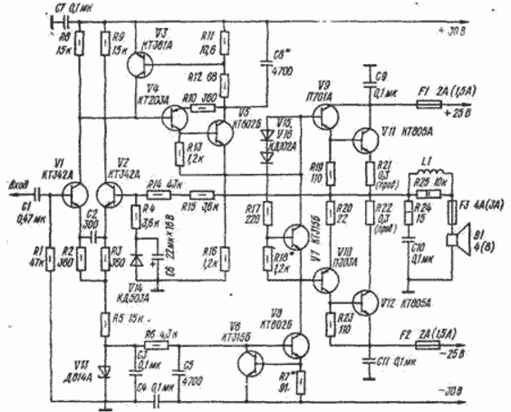
Encyclopedia of radio electronics and electrical engineering / Transistor power amplifiers The decrease in dynamic distortions in the amplifier was achieved by expanding the bandwidth of the original (without common OOS) amplifier, using linearizing local OOS and appropriately choosing the cutoff frequencies of the amplitude-frequency characteristics of the cascades. High thermal stability is ensured by local environmental protection, the use of transistors in the pre-terminal stage, the cases of which have the same thermal resistance, and a relatively large (about 250 mA) quiescent current of the transistors of the final stage.
The main parameters:
The amplifier is three-stage. The first stage is differential on transistors V1, V2, selected according to the static current transfer coefficient h21e and the emitter-base voltage. To obtain a sufficiently high input resistance, low noise level and prevent self-heating of transitions, the collector current of these transistors is chosen to be 250 μA. The total emitter current of the transistors is stabilized by the zener diode V13. Local OOS in the first stage is created by including resistors R2, R2 in the emitter circuits of transistors VI, V3. The second stage is assembled on a composite transistor V4V5. Local OOS is carried out here through the resistor R10, which connects the collector of the transistor V5 to the emitter of the transistor V4. The load of the cascade is the current generator on transistors V6, V8, the resistor R16 and the input resistance of the cascade on transistors V9, V10. The composite transistor, current generator and resistor R16 form an equivalent signal voltage source for the output stage. The resulting 100% voltage feedback eliminates the non-linearity of the current transfer coefficient and increases the cutoff frequency of the cascade. The output stage is made on transistors V9-V12. To ensure high thermal stability, P701A and P303A transistors were used in the pre-terminal stage, the cases of which have the same thermal resistance. The high quiescent current of transistors V11 and V12 reduces step-type distortion and eliminates the transient process in the main OOS loop (R15, R14, R4, C6) due to thermal shock during a sharp drop in the output signal level. Thermal stabilization of the quiescent current is carried out by the transistor V7. Diodes V15, V16 of its bias circuit are placed on the heat sink of one of the transistors of the final stage. The frequency response of the amplifier is corrected by capacitors C2 and C8 *. From a short circuit in the load and current overload, the amplifier is protected by fuses F1 - F3, transistor V3 and diode V14. Transistor V3 limits the current of the composite transistor to 9 ... 55 mA when any of the fuses blows, diode V60 limits the negative voltage at the base of transistor V14 to 2 V when fuse F0,7 blows. Transistors V5, V8 are mounted on U-shaped heat sinks bent from copper sheet 1 mm thick. Dimensions of the base of each of the heat sinks - 23 x 23 mm, shelves - 10 x 23 mm. The thermal resistance of such a heat sink is approximately 35 °C/W. The heat sinks of transistors V11, V12 are bent from copper sheet 2 mm thick. Each of them consists of two U-shaped parts, riveted at the corners of the bases with copper rivets. Base dimensions - 80 X 80 mm, shelves - 25 x 80 mm. Thermal resistance - 3,6 ° C / W. Diodes V15, V16 are glued into the holes in the heat sink of the transistor V11. Coil L1 is wound with wire PEV-2 - 0,5 turn to turn until the housing of the resistor R25 (MLT-2) is filled. The deviation of resistance from the values of all resistors indicated on the diagram, except for R24 and R25, should not exceed ± 5%. First, the part of the amplifier powered by a voltage source of ± 30 V is adjusted. To do this, remove the fuses F1 - F3, break the connection of the emitter of the transistor V5 with the base of the transistor V9, as well as the collector of the transistor V8 with the base of the transistor V10. The emitter of transistor V5 is temporarily connected to the collector of transistor V8, and the connection point of resistors R14 and R15 is connected to a common wire. By selecting the resistor R7 * (in the direction of decreasing, starting from 100 ohms), zero voltage is achieved at the collector of the transistor V8. This voltage should not go beyond ±1 V both immediately after power-up and after a ten-minute warm-up of the transistors. The symmetry of the signal limitation is checked using an oscilloscope by applying an alternating sinusoidal voltage of 100 mV to the input of the amplifier. The voltage swing at the collector of the transistor V8 must be at least ± 24 V, and the cutoff frequency must be at least 200 kHz. To check the transient response of the first two stages, the emitter of the transistor V5 is connected to the connection point of the resistors RJ4, R15 and rectangular pulses with an amplitude of 0,5 V and a frequency of 1 kHz are applied to the input. The pulses on the oscilloscope screen should have a steep (no spikes) rise and fall. If necessary, select the capacitor C8 *. After that, all connections are restored in accordance with the diagram, the fuses Fl-F3 are put in place, the coil L1 is short-circuited, a capacitor with a capacitance of 14 ... power dissipation 15...5 W. Turning on the power, measure the DC voltage at the output of the amplifier (it should not go beyond ± 10 mV), the background level (permissible range of ripples with a frequency of 8 Hz - no more than 25 mV) and the amplitude of the undistorted output signal (at a load with a resistance of 30 ohms - at least 100 V). The quiescent current of transistors V100, V300 (8 mA) is set by selecting the resistor R20 * (in the direction of decreasing, starting from 11 ... 12 kOhm). After that, the capacitor connecting the resistors R250, R18 with a common wire is removed, and the adjustment can be considered complete.
Machine for thinning flowers in gardens
02.05.2024 Advanced Infrared Microscope
02.05.2024 Air trap for insects
01.05.2024
▪ Orbital connection of qubits improves quantum computing ▪ You can go to jail for watching a pirated DVD movie in Germany ▪ New Garmin fenix 5 multisport smart watch series ▪ Renoir 7nm Desktop APUs - Ryzen 4000G, PRO 4000G and Athlon PRO 3000G ▪ Pioneer slim external burner with BDXL support
▪ section of the site Tips for radio amateurs. Selection of articles ▪ article Language is given to a diplomat in order to hide his thoughts. Popular expression ▪ article In what country did one in five people attempt suicide? Detailed answer ▪ article Securinega semi-shrub. Legends, cultivation, methods of application ▪ article Smoking substances. Simple recipes and tips ▪ TV off timer article. Encyclopedia of radio electronics and electrical engineering
Home page | Library | Articles | Website map | Site Reviews
www.diagram.com.ua |

 Leave your comment on this article: