|
|


 Arabic
 Bengali
 Chinese
 English
 French
 German
 Hebrew
 Hindi
Hindi Italian
 Japanese
 Korean
 Malay
Malay Polish
 Portuguese
 Spanish
 Turkish
 Ukrainian
 Vietnamese
|
ENCYCLOPEDIA OF RADIO ELECTRONICS AND ELECTRICAL ENGINEERING Broadband UMZCH with low distortion. Encyclopedia of radio electronics and electrical engineering
Encyclopedia of radio electronics and electrical engineering / Transistor power amplifiers Long-term operation of the power amplifier described below as part of a radio complex for playing programs from CDs and high-quality tape recordings showed that, despite the higher harmonic coefficient, the subjective quality of the output signal meets the highest requirements. Numerous listening to various musical programs at different levels of output power by the most demanding listeners did not reveal any noticeable playback errors. The advantages of the amplifier include its ability to operate at ultrasonic frequencies of the order of 100 kHz at full output power with fairly low signal distortion, extremely low distortion at low and medium frequencies, as well as relative simplicity. Main technical characteristics: Rated (maximum) power, W,
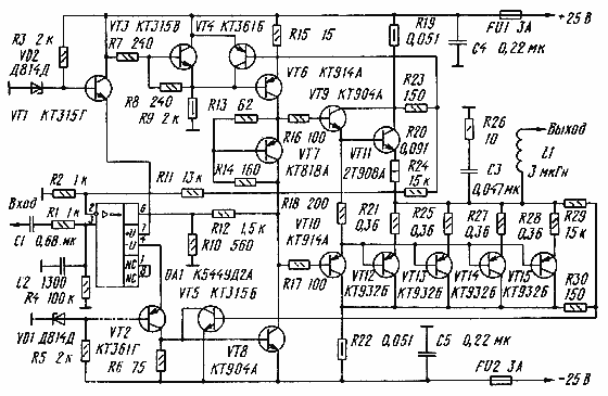
The circuit diagram of the power amplifier is shown in fig. 1. The input stage is made on the op-amp DA1. Here, also as recommended in [Dmitriev N., Feofilaktov N. OA in power amplifiers. - Radio, 1986, No. 9, pp. 42-46], its supply current is used as the output signal of the op-amp, with the only difference being that only one of the two transistors of the output stage of the op-amp works, and the second is always turned off. The output signal is taken from the negative power terminal of the op amp DA1 and, through the transistor VT2 connected according to the OB circuit, is fed to the voltage amplifier, which is made according to the usual scheme on the VT8 transistor with a current stabilizer on the VT3 and VT6 transistors. A feature of the voltage amplifier is a rather large collector quiescent current of transistors VT6 and VT8 - 40 mA. Studies have shown that as this current decreases, the distortion of the output signal begins to grow. The power dissipated by each of the transistors VT6 and VT8 is 1 W, so measures must be taken to cool them. Thermal contact between transistors VT3 and VT6 prevents an increase in the quiescent current of the voltage amplifier transistors when they are heated. To linearize this cascade, local feedback was used. The OOS voltage is removed from the collector of the transistor VT8 and through the divider R10 R12 is fed into the emitter circuit of the output transistor op-amp DA1 (pin 6).
From the output of the voltage amplifier through resistors R16 and R17, the signal is fed to the output two-stage complementary follower on transistors VT9 - VT15. In order to reduce switching distortions at high frequencies, the output follower is made on RF and microwave transistors. Since the domestic industry does not produce enough high-frequency transistors with a pn-p structure suitable for the output stage, four KT932B transistors connected in parallel with equalizing resistors in the emitter circuits are used as such. The characteristics of such a kit are in good agreement with the characteristics of the 2T908A npn transistor used in the other arm of the output stage. In order to reduce switching distortions, the resistances of the resistors in the emitter circuits of the output transistors are chosen to be sufficiently small. The amplifier is covered by a common OOS circuit (R2, R11), the depth of which at a frequency of 20 kHz is 40 dB, and at lower frequencies it exceeds 73 dB. Frequency correction in the common OOS circuit is provided by the op-amp with closed terminals 1 and 8. The amplifier protection device against short circuits in the load is made on transistors VT4, VT5 and resistors R19, R22 - R24, R29, R30. Thermal stabilization of the quiescent current of the output transistors is ensured by placing transistors VT7, VT9 and VT10 on their heat sinks. It is allowed to use the following transistors in the amplifier: VT1 - KT315 with indices B, G, D and E, VT2 - KT361 with indices G and E, VT3, VT5 - KT315 with indices B, G, E, VT4 -KT361 with the same indices, VT6 - KT914 with indices A and B and KT932A; VT7 - any pn-p or npn structure (in the appropriate inclusion) - a transistor, the housing design of which provides good thermal contact between the crystal and the heat sink; VT8, VT9 - KT904 with indices A and B. VT10 - KT914 with the same indices, VT11 - KT908A; VT12 - VT15 - KT932 with indices A and B. Only K1UD544A and KR2UD544A microcircuits can be used as op-amp DA2. If the amplifier is used or tested at ultrasonic frequencies, the resistor R26 must be replaced with a more powerful one, such as MON-2. Unfortunately, the author cannot provide a drawing of the printed circuit board, since the board was not developed specifically for this amplifier. In the author's version, a significant part of the amplifier is assembled on the heat sinks of the output transistors. Transistors VT3, VT6, VT7, VT9 and VT11 are mounted on one heat sink. On the other, transistors VT10, VT12-VT15. Resistors R7, R8, R13 - R18, R21, R25, R27, R28 are soldered directly to the terminals of these transistors. The rest of the details are located on the printed circuit board. The area of the cooling surface of each heat sink is 250 sq. cm. On a separate heat sink with a cooling surface area of 50 sq. cm, fixed directly on the printed circuit board, there are VT8 transistors of two channels of a stereo amplifier. The amplifier should be mounted in such a way that the power wires are as far away from the input circuits as possible, otherwise the distortion of the output signal will increase. Setting up the amplifier consists in setting the quiescent current of the output stage transistors within 50 ... 100 mA by selecting resistors R13 and R14 and checking the absence of high-frequency self-excitation. The resistances of resistors R16 and R17, which prevent self-excitation, depend on the current transfer coefficients of the corresponding transistors of the pre-output stage (VT9, VT10). With a transmission coefficient of these transistors of 30 ... 40, they should be equal to those indicated in the diagram, and for example, with a transmission coefficient of 120, they should be increased to 430 ohms. The two channels of the stereo power amplifier are powered by a single conventional unregulated power supply consisting of a transformer, a diode bridge, and two 8000uF electrolytic capacitors. The power transformer is wound on a toroidal magnetic circuit with a cross section of 55x21,5 mm and a window diameter of 56 mm. The network winding contains 646 turns of PEL 0,92 wire, the secondary - 104 turns of PEL 1,7 wire. The secondary winding has a tap from the middle, connected to the common wire of the amplifier. If you wish, you can try to increase the output power of the amplifier, but not more than 1,5 times, by increasing the supply voltage to +32 V. Author: A. Ivanov; Publication: cxem.net
Machine for thinning flowers in gardens
02.05.2024 Advanced Infrared Microscope
02.05.2024 Air trap for insects
01.05.2024
▪ Virtual reality cures fear of heights ▪ Simulation of human behavior in a crowd ▪ Stable atoms of pion helium obtained ▪ Nvidia AI systems for construction sites ▪ Apple is the most valuable company in history
▪ section of the site Electrician's Handbook. Article selection ▪ article Vane propeller. Tips for a modeler ▪ article What can a blue whale swallow? Detailed answer ▪ article Medical banks. Health care ▪ article Four chips. Focus Secret
Home page | Library | Articles | Website map | Site Reviews
www.diagram.com.ua |

 Leave your comment on this article: