|
|


 Arabic
 Bengali
 Chinese
 English
 French
 German
 Hebrew
 Hindi
Hindi Italian
 Japanese
 Korean
 Malay
Malay Polish
 Portuguese
 Spanish
 Turkish
 Ukrainian
 Vietnamese
|
ENCYCLOPEDIA OF RADIO ELECTRONICS AND ELECTRICAL ENGINEERING Ten teams on two wires. Encyclopedia of radio electronics and electrical engineering
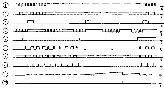
Encyclopedia of radio electronics and electrical engineering / Radio control equipment The device described below is intended for remote control of ten loads via a two-wire communication line up to 10 m long. It can be used to control household radio equipment, toys, and to transmit information about the status of sensors of various devices. This device differs from those similar in purpose by the possibility of simultaneously transmitting several commands in any combination and by the convenience of controlling the transmitted information (by the position of the knobs or switch buttons on the transmitter remote control). In addition, the transmitter does not require its own power supply - it is powered by the same communication line. The system remains operational when the supply voltage changes from 9 to 5 V, and when using K561 series microcircuits, from 12 to 5 V. The principle of operation of the device is as follows. The required commands are transmitted by setting the control panel switches to the appropriate position. In the transmitter, a cyclic poll of the state of the contactor of the console takes place with a clock frequency. A sequence of command pulses (closed contacts correspond to a short pulse, open - elongated) is transmitted over the communication line to the receiver. The receiving device processes the received information and generates a signal to turn on the corresponding loads. The schematic diagram of the transmitting device is shown in fig. 1, the receiver - in fig. 2. Fig. 3 illustrates the operation of the entire system.
After turning on the receiver with the SA1 toggle switch, the supply voltage through the communication line through the VD15 diode (Fig. 1) is supplied to the transmitter. After charging the capacitor C5 to the supply voltage, a short pulse generator with a duty cycle of 200 and a repetition rate of about 1.1 Hz, assembled on elements DD1.2, DD1, starts working. From these pulses (Diagram 3, Fig. 02.1) trigger D2 generates clock signals (Diagram 3) fed to the counter DD3. The pulses that appear sequentially at the outputs of the counter, depending on the state (diagram 1) of the command switches SA10 - SA1.3, pass or do not pass to the upper input of the element DD4 according to the scheme (diagram 2). If the contacts of a switch are open, then at the appropriate moment, pulses from the generator output arrive at the same input through the VDXNUMX diode.
A long pulse comes to the second input of the DD1.3 element from the DD2.2 trigger (diagram 5) after each contactor survey cycle. The same input from the trigger DD2.1 receives a pulse that prohibits the passage of information through the element DD1.3 in each first half of the time of polling the state of the corresponding switch. The bursts of pulses formed by the coincidence element DD1.3 after being inverted by the element DD1.4 (diagram 6) are fed to the electronic key on the transistor VT1 and then to the line (diagram 7). To ensure the selection of bursts of pulses in the receiver, the transmitter forms a pause after each polling cycle, during which the counter of the receiver is reset to zero. The receiver unit (Fig. 2), assembled on the elements DD1.1, DD1.2, is a waiting multivibrator. It is triggered by recessions of information impulses, which
come from the transmitter to the output 2 of the element DD1.1. The R1C1 circuit determines the duration of the output pulses, after which the elements DD1.3, DD1.4 and the transistor VT3 form recording pulses (Fig. 8). Information pulses (Fig. 7), inverted by the transistor VT1 (a sequence similar to Fig. 6 is obtained), are fed to the input D of triggers DD3 - OD7 (pins 5 and 9) and to the input C of the counter DD2, which, switching, allows the passage of the recording pulse to input C of the corresponding trigger. A short information pulse ends before a recording pulse is formed, and a signal 1 appears at the inverse output of this trigger, if the pulse is long, then the signal is 0. A load with a current consumption of not more than 4 ... 13 mA can be connected to the collector of each transistor VT50 - VT100 . To set the counter DD2 to its initial state, a single pulse generator is used, made on a unijunction transistor VT2. Circuit C3R5 sets the time for the formation of the installation pulse, which must be less than the pause between bursts (diag. 10). After each information message, the capacitor C3 is discharged through the diode VD) and the transistor VT1 of the transmitter (Fig. 9). The K176 series chips used in the device can be replaced with the corresponding ones from the K561, K564 series. Instead of transistors KT361 G, you can use KT361, KT347, KT3107 with any letter index. Capacitor C3 of the transmitter and C2, C3 of the receiver - K53-1A, the rest - KM, resistors - MLT. A device assembled from serviceable parts starts working immediately and does not need to be adjusted. Literature
Author: A. Kuskov, Perm; Publication: N. Bolshakov, rf.atnn.ru
A New Way to Control and Manipulate Optical Signals
05.05.2024 Primium Seneca keyboard
05.05.2024 The world's tallest astronomical observatory opened
04.05.2024
▪ USB optical replacement coming soon ▪ An effective way to clean waste water filters ▪ Stanen is a competitor of graphene ▪ Black caviar from Switzerland
▪ site section Tone and volume controls. Article selection ▪ Article Audit. Lecture notes ▪ article Where did the classic men's suit come from? Detailed answer ▪ article Japanese lacquer. Simple recipes and tips ▪ article Sim-Reader v.1. Encyclopedia of radio electronics and electrical engineering
Home page | Library | Articles | Website map | Site Reviews
www.diagram.com.ua |


 Leave your comment on this article: