|
|


 Arabic
 Bengali
 Chinese
 English
 French
 German
 Hebrew
 Hindi
Hindi Italian
 Japanese
 Korean
 Malay
Malay Polish
 Portuguese
 Spanish
 Turkish
 Ukrainian
 Vietnamese
|
ENCYCLOPEDIA OF RADIO ELECTRONICS AND ELECTRICAL ENGINEERING Touch Memory - electronic identifier. Encyclopedia of radio electronics and electrical engineering
Encyclopedia of radio electronics and electrical engineering / Radio amateur designer Introduction In systems for automatic identification of personnel, technical products, and goods, the most popular are such traditional identifiers as a bar code and a magnetic strip. However, despite their simplicity and low cost, these identifiers have a number of significant limitations. Their disadvantages include insignificant information capacity, the impossibility of promptly changing the recorded data, a greater dependence on operating conditions, and the need to use special reading devices that convert optical or magnetic signals into a digital code. The widespread introduction of information systems in production, management, the financial sector, trade, and the social sphere required the creation of more advanced means of automatic identification. These tools can rightly be attributed to a fundamentally new type of electronic identifiers of the American company "Dallas Semiconductor". The DS199X family, called Touch Memory, has a number of unique features. Touch Memory is a non-volatile memory housed in a metal case with one signal pin and one ground pin. The case, which looks like a miniature button battery, is easily attached to the product or to a carrier (card, keychain). Information is written to and read from the instrument's memory by simply touching the reader on the Touch Memory case. Memory organization The Touch Memory family includes 5 devices that are identical in case design, but differ in functionality, memory size, and method of access to it (Table 1).
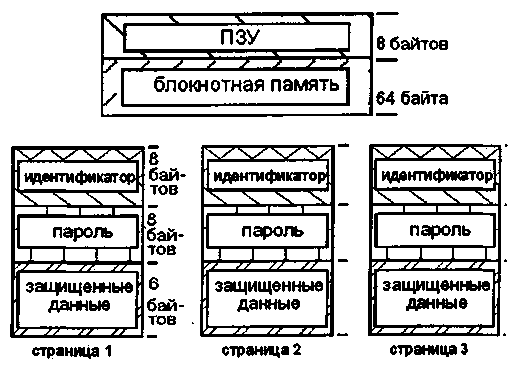
There are four main blocks in the structure of Touch Memory: read-only memory, notepad memory, random access memory, real-time clock (for DS1994), as well as a battery - a built-in miniature lithium battery (Fig. 1).
Read-only storage Each Touch Memory instrument contains read-only memory (ROM) that stores a 64-bit code consisting of an 8-bit instrument type code, a 48-bit unique serial number, and an 8-bit checksum (Figure 2).
The data placed in the ROM is a unique code combination that is written into the device using a laser installation during its manufacture and cannot be changed during the entire life of the device. During the recording and testing process at the factory, it is guaranteed that no two units will be produced with the same part number. Since when reading data from the ROM, at any time the electrical contact of the reader with the device case may be broken, it is necessary to control the integrity of the data being read. For this purpose, Touch Memory uses cyclic redundancy check (CRC). The pre-calculated checksum of the lower 7 bytes of the contents of the ROM is stored in the high byte. When reading data from ROM in the reader (personal computer, microprocessor controller), a checksum is calculated, which is compared with the control code recorded in the high byte. In the event that the codes matched, the serial number was read correctly. Otherwise, the data is re-read from the ROM. The ROM supply voltage is supplied via the data signal line, which allows, firstly, to save the energy of the built-in lithium battery, and secondly, to always read the memory regardless of the battery energy. Random Access Memory The simplest instrument of the DS1990 family contains only read-only memory. All other devices also have static random access memory. The number of write-read cycles in this memory is not limited. The memory is powered by a miniature lithium battery with a lifespan of 10 years. All RAM is divided into separate pages of 32 bytes. DS1992 has 4 pages which can store 256 bytes, DS1993 and DS1994 have 16 pages which can store 512 bytes. DS1994 contains an additional 17th page, which has a volume of 30 bytes and is intended for the operation of the real time clock (Fig. 3).
Since the data is written to the memory at the moment of touching the reader and the body of the device, the violation of the electrical contact at this moment can lead to the destruction of information in the memory. To prevent the destruction of information, the structure of Touch Memory provides additional buffer memory, which performs the function of a notepad area. This memory protects the instrument from accidentally writing new data over existing data or from writing to the wrong address. The amount of scratchpad memory is equal to the size of a page of RAM - 32 bytes for DS1992-94. Consider the principle of operation of notepad memory. All data entering the instrument is initially written to scratchpad memory. Then they are transferred from it to the reader, where they are compared with the data that needed to be written. After verification, the operation of copying the contents of the notepad memory to the main memory is performed. Since the copying is performed inside the Touch Memory, the integrity of the information is guaranteed even if the external contact is broken. Access protected RAM Devices DS 1992-94 have a RAM identical in structure, any page of which is available both for reading (directly) and for writing (via scratchpad memory). The DS 199.1 has a more complex RAM architecture. It implements at the hardware level memory protection against unauthorized access. All non-volatile memory is divided into four independent pages of 64 bytes each, one of the pages is notepad memory. Each page of the main memory consists of 48 bytes for storing data, and two service fields of 8 bytes each for storing an identifier and a password (Fig. 4).
The memory access mechanism is implemented using two keys: public, stored in the identifier field, and private, recorded in the password field. The public key is written and read, the private key is only set and cannot be read. The private key provides authorized access to memory and is protected from accidental change by the public key. During the initial formatting, the codes of the public and private keys of this page are written into the service fields of each page. Whenever memory is accessed in the DS1991, the private key of that page is first transmitted. In the event that it matches the key previously written in the password field, the memory will be available both for writing and for reading. If the codes do not match, the data is not written to the memory, and in the read mode, a sequence of random numbers is read from the DS1991. To write a new private key value to DS1991, you must pass the public key code of the selected page. If this code matches the code previously recorded in the identifier field, new values of both keys are written to the service field of this page, and the data area is erased. If the codes do not match, the value of the private key does not change. The memory access mechanism implemented in DS1991 provides reliable protection of memory from unauthorized write-read, which is extremely important in a number of applications. Real time clock The DS1994 has a real time clock circuit. The built-in miniature crystal oscillator, operating at a frequency of 32,768 Hz, produces stable timing signals - 256 pulses per second. The circuit contains three counters: a 40-bit time pulse counter, a 40-bit interval timer that counts the time the signal line is active, and a 32-bit cycle counter that counts the number of data exchange cycles with the device. The upper bytes of the time pulse counter and the interval timer provide time counting with second precision. In addition to these counters, the circuit has three registers of a similar purpose. If the current value of the counter coincides with the data previously recorded in the register, the corresponding flag is set in the status register. If at the same time the corresponding interrupt enable bit is set in the status register, then an interrupt is generated that can be read via the signal line. Single wire interface A distinctive feature of Touch Memory is the exchange protocol with the reader developed by Dallas Semiconductor. For receiving and transmitting information, one bidirectional signal line is used (the second wire is a ground contact). The exchange on one line is carried out in the half-duplex mode (either reception or transmission). The interaction of devices via a single-wire interface is organized according to the principle of "master-slave" (master-slave). In this case, the reader is always the master, and one or more Touch Memory devices are the slaves. The interaction of several devices with the reader on one bidirectional line is supported by Touch Memory hardware. The exchange protocol over a single-wire interface is two-level. At the first logical level, exchange commands with ROM and RAM are used to interact with devices (Table 2).
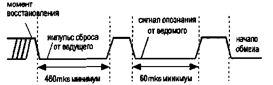
The group of ROM exchange commands consists of four commands: ROM read, skip, compare, and search. The last two commands provide interaction on one line of several Touch Memory with the reader. The compare command initiates an exchange with the device whose serial number is specified. The search command allows you to determine the serial number of one of the devices connected to the bidirectional line. Commands for exchanging with notepad and main memory are processed by Touch Memory only after the execution of one of the commands for exchanging with ROM. Thus, when several devices connected to the same line interact, the reader sends a comparison command over the line, according to which only one device is selected, which subsequently receives commands for exchanging with memory. All exchange commands have a fixed size - one byte, the data is represented by 8-bit integers. The master always initiates an exchange by sending commands to the slave. The physical layer protocol is used to transfer commands and data over a single wire interface. Commands and data are transmitted in serial code. To ensure the integrity of the transmitted information, the exchange protocol at the physical layer strictly regulates the time parameters of the signals on the line. The data exchange protocol consists of three main cycles: initialization, writing and reading. The initialization cycle is the initial cycle of any information exchange with the Touch Memory. In this cycle, the master polls the line, determining the presence of Touch Memory on it. The initialization cycle is synchronized by a negative reset pulse generated by the master. After sending the signal, the master releases the line and enters the receive mode. In the event that a Touch Memory device is connected to the line, it detects the master's clock signal and, after a temporary pause, sends him an identification signal (Fig. 5). This response signal informs the host that there is electrical contact with the Touch Memory and that the exchange can begin.
Data is transmitted over a single-wire, bi-directional line in discrete time intervals called time segments (typically around 60 µs). When transmitting data, a pulse-width coding method is used, reminiscent of Morse code: during one time segment, long or short states of a logical zero on the line determine the value of the transmitted bit. Provides data transfer rates up to 16,6 kbps. Synchronization of the time segment during recording is carried out by the negative edge of the signal that forms the master device. To transfer a logical unit to the Touch Memory, the master device releases the line after sending a clock signal; to write a logical zero, the master device maintains a low state of the line during the entire time segment (Fig. 6a). The described write cycle is repeated for each command bit transmitted.
At the beginning of the read cycle, the host device also sends a low-level clock signal to the line, after which it releases the line and enters the receive mode. Further, during the entire time segment, the state of the single-wire line is determined by the slave device - Touch Memory. In this case, a logical unit is transmitted by a high level, and a logical zero is transmitted by a low level of a single-wire line during the entire time segment. The best time for data gating by the master device is 8 µs after the start of the time segment (Fig. 6b). The reading cycle of one bit is repeated until all data has been read.
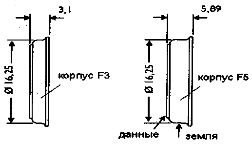
At the end of each time segment, the master device provides a pause in the exchange (recovery moment) by holding the line high. It is possible to suspend a communication session for any time between time segments, while maintaining a high state on the line. In all communication sessions, the least significant bit of data is transmitted first. Design features of Touch Memory A number of unique features of Touch Memory are provided thanks to the unusual case of the device. The memory crystal and miniature lithium battery are housed in a sealed stainless steel case with a diameter of 16 mm and a thickness of 5,8 mm (F5 case) or 3,2 mm (F3 case). The steel case is used to make electrical contacts. The case of the device is similar in design to the case of a button battery. It consists of a rim with a bottom and an electrically insulated cover. Unlike conventional microcircuits, access to the contents of the device's memory is carried out only through two lines: ground and bidirectional signal. The rim and bottom are the ground contact, and the cap acts as a signal contact (Fig. 7a). The case can withstand over 1 million mechanical connections without noticeable wear and tear.
To read data from Touch Memory devices, the Touch Probe contacting device (probe) is used, which is a mechanical assembly consisting of two stamped metal parts separated by a dielectric. The probe tip is shaped to fit exactly into the round body of the instrument. In this case, the deepened central region functions as a signal contact, and its rim serves as a ground contact (Fig. 7b).
The small size of the Touch Probe allows it to be built directly into a handheld microprocessor controller, attached to any surface, or used as a standalone handheld device. Interaction with the device is provided by a momentary touch of the probe and the Touch Memory body in such a way that the bottom of the device contacts the deep central area of the probe, and the rim contacts the side surface of the probe. The use of a simple electrical interface design ensures Touch Memory's high mechanical strength, as it has no pins or contacts that can be damaged. Reliability One of the main advantages of Touch Memory over other types of identifiers is their high reliability. Touch Memory devices withstand a mechanical shock of 500 g, a fall from a height of 1,5 meters onto a concrete floor, an 11-kilogram load on the body, are not affected by magnetic and static fields, industrial atmosphere and operate in the temperature range from -40 to +85 'C for DS 1990 and from -20'C to +85'C for all other devices of the family. Conclusion The unique design of the housing and the simple electrical interface of Touch Memory can significantly expand the scope of the electronic identifier compared to traditional means, and in some systems even replace them. The introduction of Touch Memory technology in the CIS differs significantly from the introduction of systems with conventional identifiers. If systems with magnetic cards, barcodes and more modern ones with microprocessor cards are purchased entirely abroad, then all equipment and software for systems with Touch Memory is developed and produced by domestic enterprises. This path is much cheaper and more promising, since, on the one hand, it allows using the high potential of domestic developers and easily adapting systems to the requirements of specific applications, and on the other hand, it makes it possible to make a technological leap, introducing the most advanced technology in a short time. Touch Memory devices are most widely used in control systems for physical access to premises, buildings and access to information resources, equipment, in systems of non-cash electronic payments, automatic identification of products, objects. Author: E. Zlotnik; Publication: N. Bolshakov, rf.atnn.ru
A New Way to Control and Manipulate Optical Signals
05.05.2024 Primium Seneca keyboard
05.05.2024 The world's tallest astronomical observatory opened
04.05.2024
▪ 16-bit microcontroller of the HCS12X family ▪ Barge with hydrogen electric propulsion ▪ The Milky Way is Bigger Than Thought
▪ section of the site Personal transport: land, water, air. Article selection ▪ article by Benjamin Disraeli. Famous aphorisms ▪ article Which village covers almost 10 million square meters. km? Detailed answer ▪ article Camphor Basil. Legends, cultivation, methods of application
Home page | Library | Articles | Website map | Site Reviews
www.diagram.com.ua | ||||||||||||||||||||||||||||||||||||||||||||||||||||||||||||||||||||||||||||||||||||


 Leave your comment on this article: