|
|


 Arabic
 Bengali
 Chinese
 English
 French
 German
 Hebrew
 Hindi
Hindi Italian
 Japanese
 Korean
 Malay
Malay Polish
 Portuguese
 Spanish
 Turkish
 Ukrainian
 Vietnamese
|
ENCYCLOPEDIA OF RADIO ELECTRONICS AND ELECTRICAL ENGINEERING SSTV test signal generator. Encyclopedia of radio electronics and electrical engineering
Encyclopedia of radio electronics and electrical engineering / Measuring technology Anyone who has ever had to deal with analog-to-digital technology knows how difficult it is to set it up without the appropriate instruments (oscilloscope, square-wave generator, frequency meter). SSTV equipment nodes need this setup. Vilnius radio amateur Alexander Vlasenko (UP3BD) developed a generator of test SSTV signals (similar ones are described in [1], [2], [3]). It is similar to those used in the service of household television receivers. The generator reproduces test signals of a special form in SSTV standards - a white grid, a black grid, a checkerboard, vertical and horizontal stripes, black and white fields, a gray wedge (gradation from black to white). The generator is implemented on the basis of TTL series integrated circuits, two diodes and five transistors.
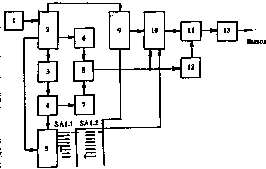
The functional diagram of the signal generator is shown in fig. 1, where the following designations are accepted: 1 - master generator;
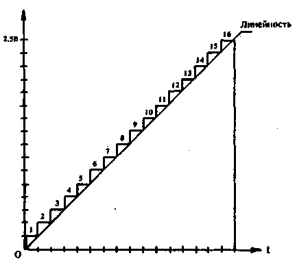
Schematic diagram of the test SSTV signal generator is shown in fig. 2. (56 Kb) The master generator is implemented on the elements of DD1.1; DD1.2; DD1.3. Actually, on the elements DD1.1 and DD1.2, an oscillator is assembled, in which positive feedback through the capacitor C1 covers two elements. Element DD 1.1 is brought into a linear amplifying mode using a negative feedback resistor R1. Element DD1.3 is used here as a buffer to reduce the effect of the load on the frequency of the generator. Capacitor C1 and resistor R1 are selected in such a way that rectangular pulses with a frequency of 1.3 Hz are obtained at the output of element DD256. These pulses from pin 8 DD1.3 are fed to the counting input of a binary counter-divider by sixteen, pin 14 DD2. From its outputs (pins 12, 9, 8, 11) binary code 1, 2, 4, 8 through the control circuit on MS DD9 is fed to the inputs of a digital-to-analog converter implemented on the elements DD10.1; DD10.2 and DD11.1; DD11.2. From output 11 MS DD2, rectangular pulses with a frequency of 16 Hz are fed to the input of a single vibrator (pin 1 MS DD7), at its output (pin 4) we get negative horizontal scan pulses SSTV normalized in duration and frequency (16 Hz - 5ms). The elements of the timing circuits MS DD7 R2 and C2 are selected in such a way that the duration of the output negative pulse is 5 ms. At the same time, a positive pulse with a duration of 5ms output 13 MC DD7, arrives at the inputs of the synchronous reset (two-input element AND, pins 2 and 3 MC DD2, prohibiting the action of pulses on the clock inputs and resetting the data on all triggers, i.e. after each sixteenth pulse of the binary counter-divider DD2 it is reset). Thus, the binary input from the output of MS DD2 through the control circuit on MS DD9 is fed to the input of the DAC (elements DD10.1; DD10.2 and DD11.1; DD11.2.). The code signal of a binary number is converted into an analog one by the resistor matrix R1...R7, respectively, according to the weight codes. At the signal summation point (emitter VT2), a periodic stepped signal is formed. The number of signal gradations is 16 (Fig.3).
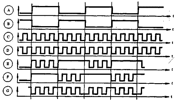
Personnel sync pulses are formed as follows. Rectangular pulses from output 11 MS DD2 with a frequency of 16 Hz are divided by dividers into MS DD3 (by 16) and DD4 (by 2 and 8). From pin 11 MC DD4, a pulse following with a period of 8s starts a single vibrator on MC DD7 (second half), at the output of which (pin 12) we get a frame pulse with a duration of 30ms. This is achieved by selecting the timing chain R3, C3. The shape shaper of the test signals is implemented on the elements of MS DDS and MS DD6. Plots illustrating its operation at various points are shown in fig. 4. The generated sequence of signals controls the operation of the control circuit on the MS DD9 (four logic elements 2OR), which, in turn, controls the operation of the DAC.
Horizontal and vertical synchronization pulses (pins 4 and 12 DD7) through the switch on the elements DD8.1; DD8.2 prohibit the operation of the DAC, open the key on the transistor VT1 and thereby connect the tuned resistor R9 to the common wire. It determines the voltage drop across the collector of transistors VT2 and VT3, which is applied to the VCO. Resistor R11 in the VT2 base circuit sets the amplitude of the linearly varying DAC voltage (Fig. 3), and R14 in the VT3 base circuit sets its linearity. The VCO itself is assembled on DD12.1 elements; DD12.2; DD12.3 and two transistors (VT4, VT5). The range of change of its frequency lies in the range from 2400 Hz to 4600 Hz - it is determined by the elements C6 and R16. On the element DD13.1, a counter-divider by two is implemented. The generated pulse-code modulated signal (PCM) from pin 6 MS DD13 is filtered by an LC low-pass filter with a bandwidth of up to 3,4 kHz. Its load is resistor R21, with which the amplitude of the output complex test signal SSTV applied to the input of the SSTV monitor is regulated. This signal can also be applied to the microphone input of the transceiver. In this case, you can give your correspondent the opportunity to set up his monitor, without having a similar generator, directly from the air. You can increase the precision of the signal generator by replacing the RC generator on the elements DD1.1; DD1.2; DD1.3 to a quartz crystal with a frequency of 256 kHz, assembled according to well-known schemes, and then divided by a divider with a division factor of 1000 (for example, three MS type K155IE 1). Setting up the test signal generator is carried out as follows. Resistor R16 (upper limit) and C6 (lower limit) set the VCO frequency range, controlling the frequency with a frequency meter at pin 8 of the DD12 MS. It should lie within 2400 ... .4600 Hz, at a voltage of 0 ... 2,5 V based on the transistor VT4. Resistor R9 sets the frequency of 2400 Hz at pin 8 MS DD12; in this case, the DAC must be given a prohibition signal from the output 8 MS D8. To do this, disconnect the outputs 1 2 and 13 MC DD1 from the outputs of the single vibrator MC DD7 and through a resistor of 1,2 kOhm from a +5 V source, a logic unit level is applied. The connection is then restored. Resistor R11 sets the amplitude of the linearly changing VCO control signal based on VT4 within +2,5 V, and resistor R14 determines the linearity of its change. Control is carried out with an oscilloscope by connecting its probe to the base of the VT4 transistor. The last step in the setup is to set the time intervals formed by the dual single vibrator on the DD7 MS. They are set by selecting RC time-setting elements, while controlling the duration of the generated negative pulse at pins 4 and 12 of the DD7 MS. For lowercase (pin 4) it should be equal to 5 ms, for personnel - 30 ms (pin 12). Since the pulse repetition period at the output of 12 MS DD7 is 8 s, it is long and inconvenient to observe it on the oscilloscope screen. Therefore, by disconnecting pin 9 of MC DD7 from pin 11 of MC DD4, connect it to pin 11 of MC DD2, set the pulse duration from the output of MC DD7 to 30 ms, then restore the connection according to the circuit diagram. The procedure for working with the test signal generator is simple. After applying a +5 V supply voltage to it, connect its output to the input of the SSTV monitor, set the test signal shape switch S1.1 and S1.2 to the gray wedge (gradation) position and resistor R21 set the signal level so that on the monitor screen there are vertical stripes are visible, changing in volume (16 in total) from white to black. Then other generated images are viewed by alternately switching switches S1.1 and S1.2. Using the described test signal generator, SSTV monitors were tuned at the stations UA2FDX, UA2FEP, UA2FGF. Literature:
Author: Kovalenko D.A. (UA2FDX) Chernyakhovsk; Publication: N. Bolshakov, rf.atnn.ru
The world's tallest astronomical observatory opened
04.05.2024 Controlling objects using air currents
04.05.2024 Purebred dogs get sick no more often than purebred dogs
03.05.2024
▪ Smart glasses Huawei X Gentle Monster EyeWear ▪ 64-layer V-NAND Flash and SSD ▪ Blue Satellite Wireless Headphones ▪ Connecting chips at unthinkable angles
▪ site section Clocks, timers, relays, load switches. Article selection ▪ Machine gun article. History of invention and production ▪ article In what animals can a severed limb try to feed the former owner? Detailed answer ▪ Behr article. Legends, cultivation, methods of application ▪ article Starch stains under the action of iodine. Chemical Experience
Home page | Library | Articles | Website map | Site Reviews
www.diagram.com.ua |

 Leave your comment on this article: