|
|


 Arabic
 Bengali
 Chinese
 English
 French
 German
 Hebrew
 Hindi
Hindi Italian
 Japanese
 Korean
 Malay
Malay Polish
 Portuguese
 Spanish
 Turkish
 Ukrainian
 Vietnamese
|
ENCYCLOPEDIA OF RADIO ELECTRONICS AND ELECTRICAL ENGINEERING 300W subwoofer amplifier. Encyclopedia of radio electronics and electrical engineering
Encyclopedia of radio electronics and electrical engineering / Transistor power amplifiers
High-power low-frequency amplifiers cannot be attributed to conventional designs, since they are inherently always quite difficult to manufacture. The slightest mistake in the assembly process leads to the fact that everything has to be started all over again, and this becomes a very expensive pleasure. The described amplifier is a fairly serious design, despite its obvious simplicity and small size. The amplifier can be assembled by an experienced radio amateur in a few hours. It is recommended to use the printed circuit board when assembling this amplifier. Do not attempt to build this amplifier if this is your first major build. The DC voltage in the circuit reaches a value of 110 V, which can lead to serious electric shock. The power dissipated by the output transistors reaches very high values, therefore, when installing them, it is necessary to carefully observe measures to ensure good thermal contact between them and the radiator. The amplifier is designed for short-term operation into a load of 4 ohms, as is usual in subwoofers. In the case of prolonged operation of the amplifier in the rated power mode, it is necessary to load the amplifier on speakers with a resistance of at least 8 ohms. At the same time, the amplifier can work efficiently for a long time and deliver power of about 150 watts. To operate in continuous mode at a rated power for a load with a resistance of 4 ohms, an additional installation of 4 more output transistors is required (2 in each arm of the amplifier). The amplifier does not have protection for the output transistors from short circuiting the output. Shorting the output will instantly destroy the output transistors. Structurally, the amplifier is located in the subwoofer housing. The amplifier maintains its performance when the power supply voltage changes by no more than ±5 V. Description The circuit diagram of the amplifier is shown in fig. one.
The amplifier is made according to the scheme that has become traditional for most modern low-frequency amplifiers: with a bipolar supply and a differential stage at the input. Chain R1, C2 serves to filter radio frequency interference. The signal is applied to the input through a non-polar capacitor C1 with a capacity of 4,7 microfarads. The impedance of this capacitance provides a small roll-off of the frequency response at very low frequencies. If you use a capacitor with a polystyrene or fluoroplastic dielectric with a capacity of 1 μF, then with a nominal input resistance of 22 kOhm, a blockage at a frequency of 7,2 Hz will be about -3 dB. The differential stage is made on transistors VT2 and VT3. Transistor VT1 performs the function of a current source. The base of the transistor VT3 is connected to the output of the amplifier through the resistor R12. As soon as a non-zero DC voltage appears at the amplifier output, the error signal amplified by the differential stage will go to subsequent stages and change their mode so that the DC output voltage becomes zero. If the parameters of the transistors VT2 and VT3 are identical, no direct current flows through the load and, therefore, an isolation capacitor in the load circuit can not be used. The low-frequency signal, amplified by the transistor VT2, is taken from the load resistor R5 and fed to the base of the transistor VT4. Further, the amplified low-frequency signal is fed to a push-pull amplifier based on transistors VT5 ... VT8. Diodes VD2 and VD3 provide the initial bias of the output stage transistors and are also placed on the radiator. They must be in good thermal contact with the amplifier heatsink. Violation of this rule will lead to the fact that the temperature regime of the output transistors will get out of control and, as a result, the output of the terminal transistors will fail due to thermal overheating. The output stage uses transistors 2SC3856 and 2SA1492. They can be replaced with cheaper MJ21193/MJ21194 or 2SC3281/2SA1302 respectively. As a VD1 LED (Fig. 1), you can use any low-power, green glow. Resistors R10, R11 and R22 film with a power of 1 W, R16 ... R21 wire with a power of at least 5 W, the rest of the film - 0,25 W. Since the output stage operates in class B mode, the amplifier has increased distortion in the high frequency region. Deep OOS in the low-frequency region makes it possible to obtain distortions at a frequency of 1 kHz of about 0,04%. With an output power of 250W, transient power peaks can reach over 300W. When using a powerful transformer in the power supply and large filter capacitance ratings, it is possible to ensure stable operation of the amplifier with an output power of up to 350 watts. In this case, the output stage must be assembled according to the circuit shown in Fig. 3 by adding 4 powerful transistors VT13...VT16 and low-resistance resistors R23...R26.
Despite the amplifier's wide bandwidth, distortion above 10 kHz is significant. When measuring peak power, the power supply voltage dropped from 56 V to 50,7 V at 8 ohms and to 47.5 V at 4 ohms. On fig. 2 is a diagram of a peak overload indicator. Laboratory measurements of the parameters of the amplifier showed the following results, shown below.
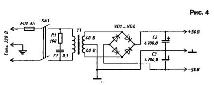
The overload indicator is designed to monitor the operating mode of the amplifier. Inputs a and b of the indicator are connected to the base circuits of the differential amplifier stage. In the linear mode of operation of the amplifier, the voltages at points a and b are equal. In the event of an overload of the amplifier, the distorted feedback signal supplied to the base of the transistor VT3 of the differential stage will differ from the input signal and an error voltage will appear at pin 1 of the DA1.1 microcircuit, which is amplified by the amplifier on DA1.2 and fed to the peak detector DA2.1 .. .DA2.2. The overload indicator is the VD3 LED - red, included in the collector circuit of the transistor switch VT1. The lighting time of the LED in the event of even a short-term error signal is determined by the time constant of the C3R12 chain. The adjustment of the indicator consists in setting the sliders of the potentiometers R5 and R9 to a position in which the VD3 LED lights up in the presence of non-linear distortion of the output signal. Power supply unit The power supply circuit is shown in fig. 4. The transformer must be used with a power of at least 400 W and an output voltage of 2 x 40 V.
Capacitor C1 must be designed for a voltage of at least 240 V, bridge rectifiers - for a current of 35 A, filter capacitors - for an operating voltage of at least 63 V, filter capacitor capacitance - 4700 ... 10000 μF. Author: ELLIOTT SOUND PRODUCTS, PO Box 233, Thornleigh NSW 2120, Australia
Machine for thinning flowers in gardens
02.05.2024 Advanced Infrared Microscope
02.05.2024 Air trap for insects
01.05.2024
▪ Epson Perfection Professional Flatbed Scanners ▪ Physical culture computer game EA SPORTS Active 2.0 ▪ Samsung Embedded Smart Home Appliances ▪ Large underwater bike park built in Amsterdam ▪ Thubber: super elastic rubber with metal properties
▪ section of the site Electronic directories. Article selection ▪ article Two-faced Janus. Popular expression ▪ article Which matches between Inter and Milan discredit the away goal rule? Detailed answer ▪ article Guatemalan indigo. Legends, cultivation, methods of application ▪ article Magic photos. Focus Secret
Home page | Library | Articles | Website map | Site Reviews
www.diagram.com.ua |

 Introduction

 Leave your comment on this article: