|
|


 Arabic
 Bengali
 Chinese
 English
 French
 German
 Hebrew
 Hindi
Hindi Italian
 Japanese
 Korean
 Malay
Malay Polish
 Portuguese
 Spanish
 Turkish
 Ukrainian
 Vietnamese
|
ENCYCLOPEDIA OF RADIO ELECTRONICS AND ELECTRICAL ENGINEERING Transceiver Radio-76. Encyclopedia of radio electronics and electrical engineering
Encyclopedia of radio electronics and electrical engineering / Civil radio communications The transceiver is designed to operate on SSB (lower sideband) in the telephone section of the 80-meter amateur band. It has the following characteristics: range of received and emitted frequencies - 3,6-3,65 MHz: receiver sensitivity (with a signal-to-noise ratio of 10 dB) - no worse than 1 μV; suppression of the image channel at reception - not less than - 40 dB; "clogging" (in relation to the level of 10 μV) - not worse than 500 mV; mutual modulation (with respect to 1 μV) - no worse than 80 dB; input impedance of the receiver-75 bm; output impedance of the bass amplifier - 10 ohms; maximum output voltage LF (with AGC system running) -0,8 V; change in the output signal level (when the input level changes by 60 dB) - no more than 6 dB; local oscillator frequency instability (for both receiving and transmitting paths) - no worse than 300 Hz / h; peak output power - 5 W; the level of out-of-band radiation - no more than -40 dB; carrier suppression - not less than -50 dB; transmitter output impedance - 75 Ohm; supply voltage-12 V; quiescent current in receive mode - 200 mA; quiescent current in transmission mode - 360 mA. Single-signal receiver selectivity (non-working sideband suppression) and passband ripple are determined by an electromechanical filter. Typical when using a standard electromechanical filter EMF-9D-500-ZV will be the following values of these parameters: -6 dB level bandwidth - 2.95 kHz, -60 dB level bandwidth - 4,85 kHz, passband ripple - no more than 1,5 dB. The transceiver (without power supply) is made on three integrated circuits, 11 transistors and 19 semiconductor diodes. It is assembled according to a scheme in which the intermediate frequency amplifier path is fully used both for reception and transmission. Such a solution, in combination with the use of ring mixers, which are also fully used for reception and transmission, makes it possible to significantly simplify the circuit to the point that all low-signal paths of the transceiver for reception and transmission can be made common. In the described design, the functions of only low-frequency amplifiers (low-frequency amplifier of the receiver and microphone amplifier of the transmitter) are separated. The latter led to the use of several additional components, but it significantly simplified switching. Another feature of the transceiver is the non-traditional construction of the receiving path (without a high-frequency amplifier, with a ring mixer at the input). This made it possible to obtain good characteristics for "clogging" and for mutual modulation. Despite the absence of an RF amplifier and the use of a passive mixer, it was possible to obtain a sensitivity of about 1 μV, more than sufficient for operation on the 80 m band.
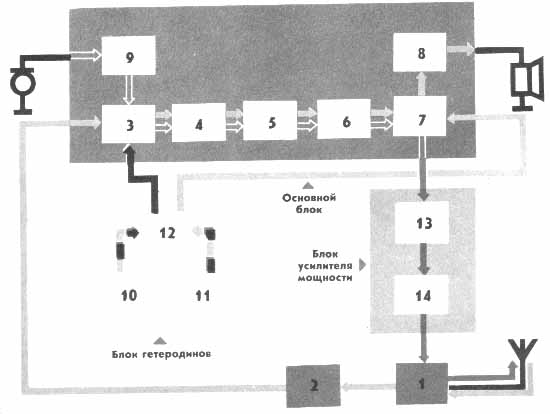
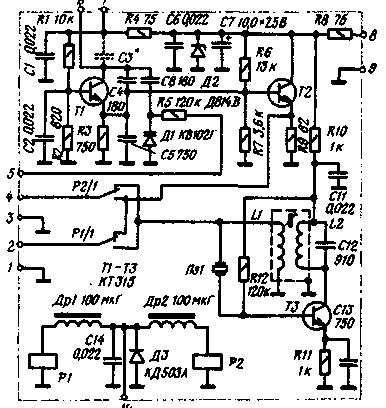
The transceiver consists of three blocks (main, local oscillators and amplifier). In the receive mode, the signal through the antenna switch 1 and the lumped selection filter 2 is fed to the first annular mixer 3 located in the main unit. From the block of local oscillators to this mixer through the switch 12, the voltage of the high-frequency local oscillator 10 is supplied with a frequency lying in the range of 4,1-4,15 MHz. The intermediate frequency signal (4 kHz) amplified by the first stage of the IF amplifier 500 passes through the electromechanical filter 5, is amplified by the second stage of the IF amplifier 6 and enters the second ring mixer 7, which performs the functions of a mixing detector in this mode. From the local oscillator board through the switch 12, a voltage with a frequency of 500 kHz is supplied to it from the local oscillator 11, and the detected signal is fed to the LF amplifier 8. In the transmission mode, the signal from the microphone is amplified by a low-frequency amplifier 9 and fed to the first ring mixer 3, which in this mode performs the functions of a balanced modulator. From the local oscillator block, the voltage of the local oscillator 12 is supplied to it through the switch 11. The first stage of the IF amplifier amplifies the DSB signal. An electromechanical filter extracts the upper sideband from this signal, and the generated SSB signal, after amplification by the second stage of the IF amplifier, is fed to the second ring mixer, which is supplied with a local oscillator voltage 10 with a frequency of 4,1-4,15 MHz (through switch 12). The converted signal is amplified by a power amplifier, consisting of preliminary 13 and final 14 amplifiers, and through switch 1 enters the antenna. Schematic diagrams of the main unit, the local oscillator unit and the power amplifier unit are shown in fig. 1, 2 and 3. In the receive mode, the first ring mixer on diodes D1-D4 (Fig. 1) receives a signal through pins 9 and 10, and a local oscillator voltage with a frequency of 7-8 MHz through pins 4,1 and 4,15. At the output of the ring mixer, an intermediate frequency signal (500 kHz) is allocated, which is amplified by an IF amplifier made on the transistor T1. The preliminary filtering of the IF signal is carried out by the oscillatory circuit L2C4C5C6, and the main one is the electromechanical filter F1, included in the collector circuit of the transistor T1. To further amplify the signal in the IF path, an MC1 microcircuit was used, which is a conventional cascode amplifier (See "Radio", 1975. N 7. p. 55.).
The signal selected on the oscillatory circuit L3C15 is fed to the second annular mixer on diodes D9-D12. Through conclusions 12 and 13, a voltage with a frequency of 500 kHz is supplied to it from the local oscillator block. The low-frequency signal passed through the low-pass filter Dr2S21R14C22 is amplified by the MS2 microcircuit, which is a two-stage amplifier with direct connections, and transistors ТЗ-Т5. To terminals 16 and 17, you can connect a loudspeaker with a resistance of 5-10 ohms or headphones (preferably low-impedance). In transmit mode, the signal from the microphone is fed to pin 1 and amplified by the MC3 chip. This microcircuit (unlike MC2) is not usually turned on: its output 10 is connected through an electrolytic capacitor not to the case, but to output 11 (microcircuit), from which the output signal is taken. At the same time, its gain and output impedance decrease (up to about 300 ohms). From the microphone amplifier, the low-frequency signal is fed to the first ring mixer, which now functions as a balanced modulator. A voltage with a frequency of 8 kHz is applied to this mixer through pins 9 and 500 from the local oscillator unit. The mixer is balanced with a trimming resistor R2. From the balanced DSB modulator, the signal enters the IF path, from the output of which the already formed and amplified SSB signal is fed to the second ring mixer. Through pins 12 and 13, this mixer receives a local oscillator voltage with a frequency of 4,1-4,15 kHz. The converted signal through pins 14 and 15 is fed to the power amplifier for filtering and amplification. From pin 18, the signal can be applied to VOX, and from pins 16 and 17 - to ANTI-TRIP. The block provides the possibility of automatic gain control of the IF path both during reception (ARC) and during transmission (ALC). This adjustment is carried out in the second stage of the IF amplifier (microcircuit MC1) by the auxiliary transistor T2. Control signals are fed to the base of the transistor through decoupling diodes D14 and D15 (pins 3 and 4}. Manual gain control is available only in receive mode. It is carried out by applying a bias voltage through terminal 6 of the block to the transistor of the first stage of the IF amplifier. The only node in the main unit that is switched during the transition from reception to transmission also belongs to this cascade. How it works will be discussed below. In the block of local oscillators (Fig. 2) there is a switch on the relays P1 and P2 and two generators. One of them is a smooth range generator (GPA). changing the frequency of which is tuned to the operating frequency. It is made on the transistor T1.
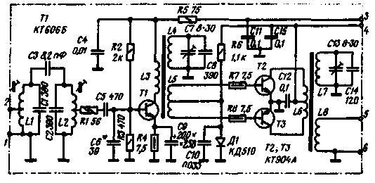
A buffer stage is assembled on transistor T2. The inductor of the oscillatory circuit of the generator is located outside the board and is connected to it through pins 6 and 7. This solution will allow in the future, when transferring the local oscillator board to the transceiver of the first category, it is easy to change the operating frequency range of the local oscillator. without making changes to the board itself. The frequency of the GPA is changed by the D1 varicap, applying a control voltage to it through the output a. The second generator (at a frequency of 500 kHz) is made on a transistor T3. Its frequency is stabilized by a Pe1 quartz resonator. The position of the relay switch contacts in the figure corresponds to the receive mode (the relay is not energized). Through pins 1 and 2, the voltage from the local oscillator unit is supplied to the first mixer (pins 7 and 8 of the main unit), and through pins 3 and 4 to the second mixer (pins 12 and 13 of the main unit). The control voltage to the relays P1 and P2 is supplied through pin 10, and the supply voltage to the local oscillator unit is fed to pins 8 and 9.
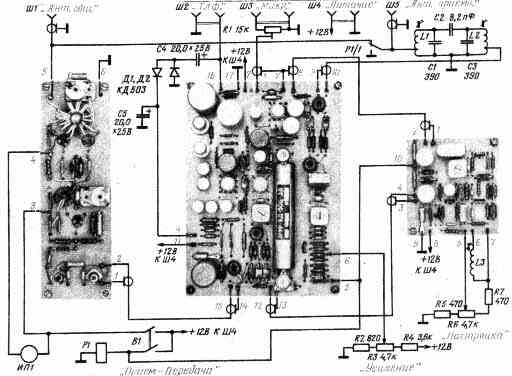
In the transmission mode, the signal from the main board goes to pins 1 and 2 of the power amplifier board (Fig. 3). The band-pass filter L1C1C3L2C2 selects from the incoming signal a useful signal that lies in the operating frequency band of the transceiver. The first stage of the power amplifier (transistor T1) operates in class A mode, and the final stage, made according to a push-pull circuit on transistors T2 and T3, operates in class B mode. The bias to the transistors sets the stabilizer on diode D.1. The output signal to the antenna is taken from the coupling coil L8 (through pins 5 and 6). Power is supplied to the first stage through pin 3, and to the final stage through pin 4. The connection diagram of the transceiver blocks and parts installed outside these blocks is shown in fig. 4 in the text. For the blocks in this figure, photographs of their printed circuit boards are given. The antenna is connected to connector Ш1 and through the contacts P1 / 1 of the antenna relay, the received signal is fed to the double-circuit band-pass filter L1C1C2L2C3. From the filter, the signal is fed to the main unit. Through connector Ш5 it is possible to connect a separate receiving antenna, bypassing the antenna switch. With a variable resistor R6, the transceiver is tuned to the operating frequency, and with a resistor R3, the gain of the IF path is changed upon reception.
Diodes D1, D2 and capacitors C4, C5 form a voltage doubling rectifier that generates the AGC control signal. Switch B1 switches the transceiver from the "Receive" mode to the "Transmit" mode. In the diagram, it is shown in the "Receive" mode position. In the "Transfer" mode, power is supplied through the upper contacts of the switch to the power amplifier unit, and through the lower contacts - +12 V voltage to the PI relay of the antenna switch, the PI and P2 relays of the switch located in the local oscillator unit (Fig. 3), and to the output 5 main unit. Let us analyze the principle of switching during the transition from reception to transmission in the first stage of the IF amplifier of the main unit (Fig. 1). In the "Reception" mode, the lower output of the resistor R6 according to the circuit is connected to the case through the winding of the relay P1 (Fig. 2), the diode D7 is open by the voltage falling on the resistor R5. Capacitor C9 connected in parallel with resistor R5. reduces negative AC feedback. The amplification of the cascade in this case is maximum. When a DC voltage of +5 V is applied to pin 12, diode D7 closes, disconnecting capacitor C9 from resistor R5. The gain of the cascade decreases abruptly. This avoids overloading the IF path with the relatively large signal entering the path from the ring mixer in transmit mode. The R6D6D5 chain provides a supply to the base of the transistor T1 in the transmission mode of a constant bias that does not depend on the voltage at pin 6. that is, on the setting of the IF gain level in the receive mode. The signal from the microphone comes through connector Ш3. The trimmer resistor R1 sets the required level of this signal. The IP1 device controls the current consumed by the final stage of the power amplifier. Headphones or a loudspeaker are connected to connector Ш2. The transceiver is powered by a stabilized power source through connector Ш4. Most of the details of the transceiver are located on three printed circuit boards corresponding to its three blocks: main, local oscillators and power amplifier. Photos of these printed circuit boards are shown in fig. 4. The boards are made of one-sided foil fiberglass with a thickness of 1,5-2 mm. Pieces of silver-plated or tinned copper wire 1,2-1,5 mm thick are used as board leads. On fig. 5 shows the PCB of the main unit, in fig. 6 - block of local oscillators. Before installing the microcircuit, its leads are shortened to 10 mm and carefully tinned, always using a heat sink (tweezers, duck nose pliers). Then the leads are inserted into the holes of the printed circuit board and, after making sure that the leads are not mixed up, they are unsoldered. Particular attention should be paid to this operation, since due to the large number of pins, it is quite difficult to unsolder an incorrectly installed microcircuit, especially if you do not use special nozzles for a soldering iron. Moreover, in the absence of experience, reinstalling the microcircuit can damage the printed conductors or the microcircuit itself. The printed circuit boards of the main unit and the local oscillator unit, intended for use in a multi-band transceiver, are designed for the following details: resistors (except for the R2 resistor in the main unit) - MLT-0,25; resistor R2 in the main unit - SP4-1; fixed capacitors (except electrolytic) - KM-4 and KM-5, electrolytic capacitors - K50-6; high-frequency chokes - DM-0,1, relays - RES-15 (passport RS4.591.004), inductors in the IF amplifier and in the local oscillator at 500 kHz - FFC-2 transformers from the Selga-404 radio receiver; quartz resonator Pe1 - in case B1. Some other types of components can also be used without altering the boards. So, instead of the SP4-1 resistor, SPO-0,5 can be used, the KM-4 and KM-5 capacitors used in decoupling circuits can be replaced with KLS and KLG, and in other circuits with CT or KSO. As inductors in IF amplifiers and a 500 kHz local oscillator, with a corresponding slight correction of printed conductors, IF transformers from any transistor receivers with a turns ratio from 20:1 to 10:1 can be used. KT315 transistors can be with any letter index. You can also use any silicon high-frequency npn transistors (KT301, KT306, KT312). It should only be taken into account that as T1 and T2 of the main unit, it is necessary to use transistors with Vst> 80, and T3 (main unit), T1 and T2 (local oscillator unit) - with Vst> 40. Transistors GT402 and GT404 can be replaced, for example, with transistors MP41 and MP38. However, in this case, a low-resistance load (with a resistance of about 10 ohms) can only be switched on through a step-down transformer. Microcircuits K1US222 and K1US221 can be used with any letter indices, but then it is necessary to select resistors in the power circuits so that the voltage on the microcircuit does not exceed the maximum allowable. If a radio amateur does not have microcircuits, their analogues can be made - modules on transistors KT301, KT306, KT312, KT315. The modules should be shaped to fit on the board instead of the chip. Diodes KD503 in auxiliary circuits can be replaced by almost any silicon or germanium high-frequency diodes with low reverse currents (for example, D9K). Modern high-frequency diodes (KD503, KD509, GD507) are best suited for ring mixers, however, quite satisfactory results are obtained when using diodes D18, D311, etc. In this case, however, the sensitivity of the receiver will deteriorate somewhat (up to 1,5-2 µV), but other characteristics will not change. Varicap KB 102 can be replaced with D901 or D902. Transformers Tr1-Tr4 of ring mixers are wound on K7X4X2 cores made of 600NN ferrite. You can also use ferrite rings with a permeability of 400-1000 and an external diameter of 7-12 mm. Each winding contains 34 turns of PEV-2 0,15 wire. Transformers are wound with three wires at once, which are pre-twisted into a bundle. You should be careful when desoldering the windings of transformers (the beginnings of the windings are marked in Fig. 1 and Fig. 5 with dots). The coil L4 of the smooth range generator is wound on a frame with a diameter of 12 mm made of PTFE or polystyrene. It has 33 turns of PEV-2 0,35 wire. Winding ordinary, coil to coil. The coil is equipped with a tuning carbonyl core SCR-1. Its inductance is about 9 μH. The coils L1, L2 of the input band-pass filter are wound on frames from the KB circuits of the Speedol receiver. They contain 25 turns of dense ordinary winding with PELSHO 0,1 wire (removal from the 4th turn, counting from the grounded output). The inductance of the coils is about 6,2 μH. The power amplifier block is not designed for use with a multi-band transceiver, so it is not described in detail. It uses the same details as the other two blocks. Trimmer capacitors - 1KPVM-1. The input bandpass filter L1C1C2L2C3 is similar to the FSS used in the receive path. Coils L3-L5 are wound on a K 12X6X4 ring made of M20VCh2 ferrite and have 2, 17 and 2 (with a tap in the middle) turns of wire PEV-2 0,35, respectively. For winding coils L6-L8, a K20X10X5 ring made of M50VCh2 ferrite was used. They contain, respectively, 2 (with a tap in the middle), 16 and 2 turns of wire PEV-2 0,35. Diode KD510 (D /) can be replaced by any silicon. Parts installed by the method of hinged mounting on the chassis (see Fig. 4) can be of any type. The exceptions are relay P1 (RES-15, passport RS4.591.004) and variable resistor R6. This resistor must be of high quality. The instability of the resistance, the unevenness of its change will significantly impair the operation of the transceiver. Of the available parts, the best for this application are the SP1 resistors, which have already been in operation for some time ("lapped"). Measuring device IP1 - with a total deviation current of 0,5-1 A. One of the possible layout options for the transceiver is shown in Fig. 7.
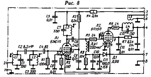
The transceiver case is formed by two U-shaped parts, one of which is the base, and the other is the cover (not shown in the figure). A flat metal chassis 1 is fixed on the base 3 with the help of racks 5 10-2 mm high. The boards of the main unit 6, the local oscillator unit 12 and the power amplifier 4 are installed on the chassis. rectangular holes with dimensions somewhat smaller than the dimensions of the boards). The power amplifier transistors are mounted on a radiator 5, which is a 5-10 mm thick duralumin plate. An amplifier board is attached to the radiator on four racks. On the rear wall of the base of the transceiver there are connectors for connecting external devices: 7 - a common antenna for the receiving-transmitting path; 8-headphones or loudspeaker; 9 - microphone; 10 - power supply; 11 - a separate receiving antenna. Variable resistors 14 are fixed on the front wall of the base of the transceiver, with which the tuning to the operating frequency is carried out, and 15, which serves to adjust the gain of the receiver, as well as the switch 16 "Reception - transmission" and the measuring device 17 to control the current of the final stage of the power amplifier. The transceiver is powered from a separate stabilized source that provides +12 V at the output at a current of up to 1 A. The establishment of the transceiver begins with setting the operating modes of the transistors T1 and TK in the main unit. To do this, switch B1 (see Fig. 4) sets the "Reception" mode, and the slider of the variable resistor R3 is transferred to the extreme right (according to the diagram) position. By selecting resistor R4 in the main unit, the voltage at the emitter of transistor T1 is about 2 V. Then, by changing the resistance of resistor R16, the voltage at the emitters of transistors T4 and T5 is set to approximately 6 V. After that, they start setting up the local oscillator block. A high-frequency voltmeter with a measurement limit of 4 V is connected to terminal 1 of the board and, by rotating the tuning core of coil L2, an RF voltage with an amplitude of about 0,5 V is achieved. Then the RF voltmeter is connected to terminal 2 and the operation of the smooth range generator is checked. The required overlap - from 4,1 to 4,15 MHz (with a margin of about 5 kHz at the edges) is set by selecting resistors R5 and R7 (see Fig. 4) and adjusting the L3 coil core. If necessary, an additional capacitor can be introduced into the local oscillator block (C3 in Fig. 2). It is installed between terminals 6 and 7 of the local oscillator board. The amplitude of the RF voltage at pin 2 should be approximately equal to 1,2 V. Rotating the "Settings" knob, check the unevenness of the local oscillator voltage over the range. It should not exceed 0,1 V. Now you can start setting up the radio frequency path - the main unit of the transceiver. A load is connected to connector Ш2 - a loudspeaker with a resistance of 6-10 Ohms or its equivalent - a resistor with the same resistance and a dissipation power of 0,5 W. In parallel with the load, an AC voltmeter or an oscilloscope is turned on. Pin 4 of the main board is temporarily shorted to ground, thereby disabling the automatic gain control circuit. At this stage of tuning, it is advisable to turn off the smooth range generator as well. By touching pin 4 of the MC2 chip with a finger or a screwdriver, they are convinced that the bass amplifier is working by the appearance of a background at the output. A standard signal generator is connected in parallel with the L4 coil. Having set the signal level to 20-50 mV, the GSS frequency is changed in the region of 500 kHz until a signal appears at the output of the bass amplifier. Without changing the settings of the GSS, reduce the level of its signal to 20 μV and connect the GSS in parallel with the capacitor C11. By rotating the tuning core of the inductor L3, they achieve the maximum voltage at the output of the bass amplifier. Then the GSS is connected in parallel with the L1 coil and the L2 coil is also adjusted to the maximum output voltage. With this setting, the GSS signal level is gradually reduced to 1-2 μV. If a radio amateur has a 500 kHz sweep frequency generator at his disposal, then capacitors C8 and SI can be selected for the least unevenness in the passband (contrary to popular belief among radio amateurs, these capacitors have practically no effect on insertion loss). It is possible to perform such a tuning without a GKCH only with a highly stable GSS. Due to the steepness of the slopes in the dips of the EMF frequency response, the signal at the transceiver output can change by 3-6 dB only due to the unstable operation of the GSS (it is enough that its frequency drifts by 100 Hz during tuning). To adjust the input and output of the EMF using the GSS, the frequency is set at a point corresponding to one of the dips in the amplitude-frequency characteristic, and by selecting capacitors C8 and SI (it is useful to temporarily connect tuning capacitors), the maximum voltage at the output of the bass amplifier is achieved. The ripples in the passband presented in the first part of the article correspond to the case of optimal tuning of the EMF input and output circuits. With serviceable parts and losses in the EMF no more than 6 dB, the sensitivity of the path from the L1 input should turn out to be no worse than 0,5 μV. Since in amateur conditions it is difficult to measure sensitivity better than 1 μV due to signal leakage, the operation of the path should be considered normal if, at a GSS signal level of 1 μV, the signal significantly (10 or more times) exceeds the noise. In the absence of a signal, the noise level at an 8 ohm load of the bass amplifier should be no more than 10 mV. By turning on the smooth range generator, tune the input FSS of the receiver. To do this, a signal from the GSS with an amplitude of 5-10 μV and a frequency of 3,625 MHz is fed to the receiver input and the transceiver tuning knob is rotated until a signal with a frequency of about 1 kHz appears at the output of the receiver's bass amplifier. The FSS circuits L1C1 and L2C3 (Fig. 4) are adjusted to the maximum voltage at the output of the bass amplifier. In the process of tuning the radio frequency path, it is necessary to ensure that the stages of the IF and LF amplifiers are not overloaded. In practice, this means that the voltage at the output of the bass amplifier in any case should not exceed 2-3 V. At the end of the tuning of the radio frequency path in the "Reception" mode, the transceiver scale is calibrated. Setting up the transceiver in the "Transmission" mode also begins with the main unit. Power is not supplied to the power amplifier at the initial stage of setup. A microphone is connected to the ShZ connector, which the radio amateur intends to use with the transceiver in the future. A millivoltmeter or an oscilloscope is connected to the output of the MC3 chip. Saying a long "A" (the distance to the microphone and the volume level should be the same as they will be in the future when working on the air), the tuning resistor R1 (Fig. 4) sets the signal level at the output of the MC3 chip to 0,1-0,15, 15 V. After that, a piece of wire is connected to terminal 2 of the main unit board and the generated SSB signal is listened to on the auxiliary receiver. The maximum carrier suppression is set using the trimmer resistor RXNUMX, The power amplifier is configured separately. After applying power to it, set the mode of the transistor T1. The current through the transistor should be approximately 50 mA. It is controlled by the voltage drop across the resistor R4, included in the emitter circuit of the transistor T1. Then, an antenna equivalent is connected to connector Ш1 (a resistor with a resistance of 75 ohms and a dissipation power of about 5 W). It can be made up of several larger resistors connected in parallel, for example, of three MLT-2 resistors with a resistance of 220 ohms each. A signal with a frequency of 2 MHz and an amplitude of 3,625-0,1 V is supplied to output 0,15 of the power amplifier board from the GSS. By connecting an RF voltmeter to the base of the transistor T1, set up the band-pass filter L1C1C2L2C3, Then, by turning on the voltmeter in parallel with the antenna equivalent, sequentially tune the oscillatory circuits L4C7C8 and L7C13C14. During the tuning process, the value of the GSS signal is gradually reduced to 20-30 mV. The tuning is completed by selecting the optimal connection with the antenna by changing the number of turns of the L8 communication coil. The tuning criterion is a doubling of the transmitter output voltage when the antenna equivalent is turned off. When a signal is applied from the GSS, the current consumed by the final stage should be 0,5-0,7 A. Having restored the connection between the main board and the power amplifier board, the transceiver is checked for transmission as a whole. The signal is listened to on the auxiliary communication receiver. Unlike the main unit and the local oscillator unit, more scarce components are used in the power amplifier. This was caused by the desire to create an all-semiconductor transceiver with an output power of 5 watts. Attempts to use less scarce transistors in the power amplifier were not successful. In the event that the radio amateur does not get the KT606 and KT904 transistors, he can make a lamp power amplifier. The scheme of such an amplifier is shown in fig. 8. When used with the described main unit, just like a solid-state power amplifier, it provides a peak output power of about 5W.
An RF signal is supplied to pin 2 from the main unit, to pins 3 and 4 - a voltage of +290 V, to pin 7 - an alternating voltage of 6,3 V. Pins 5 and 6 are designed to connect an antenna. The supply voltage to terminal 4 is supplied through a measuring device with a full deviation current of 70-100 mA. The control scheme of the transceiver remains virtually unchanged. With a tube power amplifier, the upper contacts of switch B1 (Fig. 4) are used to supply + 290 V to the power amplifier unit, and the lower ones to supply + 12 V to the remaining transceiver units. Authors: B. Stepanov (UW3AX), G. Shulgin (UA3ACM), Moscow; Publication: N. Bolshakov, rf.atnn.ru
A New Way to Control and Manipulate Optical Signals
05.05.2024 Primium Seneca keyboard
05.05.2024 The world's tallest astronomical observatory opened
04.05.2024
▪ Electronic map of pastures of Kyrgyzstan ▪ External SSDs up to 2TB Samsung T5 ▪ Graphene on platinum surfaces defies Coulomb's law
▪ section of the site Power supply. Article selection ▪ article Miserly knight. Popular expression ▪ article How deep do plant roots penetrate? Detailed answer ▪ article Seller of manufactured goods department (section). Standard instruction on labor protection ▪ article Magic envelope. Focus Secret
Comments on the article: Grysh In the GPA circuit, there is no isolation capacitor between the emitter T1 and the base T2.
Home page | Library | Articles | Website map | Site Reviews
www.diagram.com.ua |


 Leave your comment on this article: