|
|


 Arabic
 Bengali
 Chinese
 English
 French
 German
 Hebrew
 Hindi
Hindi Italian
 Japanese
 Korean
 Malay
Malay Polish
 Portuguese
 Spanish
 Turkish
 Ukrainian
 Vietnamese
|
ENCYCLOPEDIA OF RADIO ELECTRONICS AND ELECTRICAL ENGINEERING Radio control equipment for models. Encyclopedia of radio electronics and electrical engineering
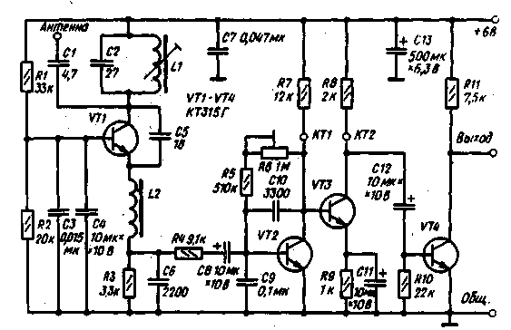
Encyclopedia of radio electronics and electrical engineering / Radio control equipment To transmit commands, a number-pulse code is used. The transmitter encoder is built on two microcircuits of the K561 series (Fig. 1). The transmitter generator is assembled according to the simplest circuit with quartz frequency stabilization on a VT2 transistor. The oscillatory circuit L1C3 is tuned to the frequency of the quartz resonator, equal to 27,12 MHz.
The transmitter does not provide special measures to match the oscillatory circuit of the transmitter with the antenna, therefore, the radiated power of the transmitter is small, and the range of the radio control system is 5 ... 10 m. To increase the range, you can increase the transmitter supply voltage to 9 V and apply a matching CLC circuit and extension coil. The diagram of the receiver of the radio control system is shown in Fig.2. The input stage of the receiver is assembled according to the scheme of a super-regenerative detector in the transistor VT1. The super-regenerator has remarkable properties - high sensitivity, low
the dependence of the output signal level on the input level, simplicity, however, it also has disadvantages - low selectivity, signal radiation, as a result of which it works as a low-power transmitter and can interfere with other receivers. The operation of the super-regenerative detector is described in many radio control books and is not covered here. On the load resistor R3 of the input stage, in addition to the useful signal, sawtooth damping pulses with a frequency of 40 ... 60 kHz are distinguished, the R4 C9 circuit is used to filter them, and the capacitor C10 serves the same purpose. The same elements suppress short-term impulse noise (for example, from the electric motors of the model) and partially the noise of the super-regenerative detector. An approximate form of the useful signal on the collector of the transistor VT2, operating in the linear amplification mode, is shown in the first diagram in Fig. 3. This signal is still far from the bursts of pulses required for the operation of the decoder. To obtain a good rectangular pulse shape, an amplifier-shaper on a VT3 transistor is used. In the absence of a useful signal, when there is a noise signal of a small amplitude super-regenerator on the collector of transistor VT2, transistor VT3 is in a state of shallow saturation, the voltage between its collector and emitter is 250 ... 300 mV and it does not amplify the input signal. Such an operating point of the transistor VT3 is set by a trimmer resistor R6.
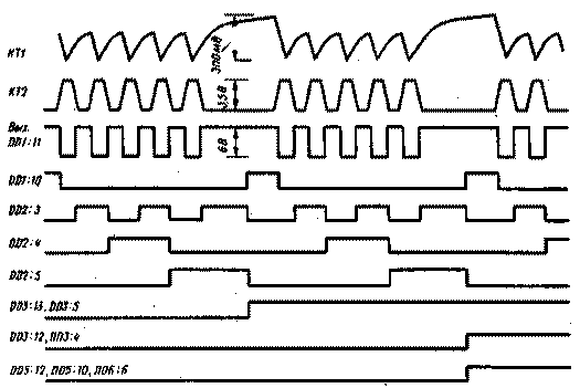
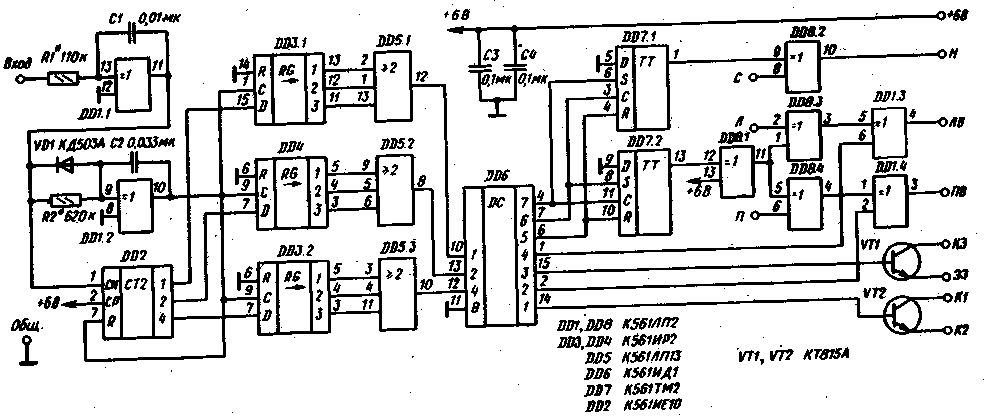
When bursts of RF pulses appear, the super-regenerative detector sends bursts of positive polarity pulses to the base of the transistor VT2, signals appear on the collector VT2 and the base VT3 in accordance with the first diagram in Fig.3. The negative half-wave of the signal closes the transistor VT3, and pulses of positive polarity are formed on its collector, opening the key stage on the transistor VT4. On its collector, bursts of pulses of negative polarity with an amplitude equal to the voltage of the power source are formed, they are fed to the input of the command decoder. The diagram of the command decoder is shown in Fig.4. Packets of input pulses of negative polarity are fed to part of the decoder on the DD1 and DD2 microcircuits. After receiving the next burst of pulses, the counter DD2 is set to a state corresponding to the number of pulses in the burst. As an example, Fig. 3 illustrates the operation of the counter in the case of receiving bursts of five pulses. By the end of the pack, a log appears at the outputs 1 and 4 of the counter. 1, at the output 2-log.0 (diagrams DD2:3, DD2:4, DD2:5 in Fig. 3). The front of the pulse from the pause detector DD1.2 rewrites the state of the counter in the shift registers DD3.1, DD4, DD3.2, as a result of which a log appears at their outputs 1, respectively. 1, log.0, log.1.
After the end of the second burst of five pulses, the pulse from the output of the pause detector DD1.2 shifts the previously recorded information from bits 1 of the shift registers to bits 2, and in bits 1 it writes the result of counting the number of pulses of the next burst, etc. As a result, with continuous reception of bursts of five pulses, all outputs of the shift registers DD3.1 and DD3.2 will be log.1, all outputs DD4 - log.0. These signals are fed to the inputs of the majority valves of the DD5 microcircuit, signals corresponding to the input appear at their outputs, they come to the inputs of the DD6 decoder. Log.5 appears at output 1 of the decoder, which is a sign of receiving a command with a number of pulses equal to five. This is how signals are received in the absence of interference. If the level of interference is strong, the number of pulses in the burst may differ from the required one. In this case, the signals at the outputs of each of the shift registers will differ from the correct ones. Suppose that when receiving one of the bursts, instead of five, the counter will count six pulses. After receiving two bursts of five pulses and one of six, the status of the outputs of the registers DD3.1, DD4 and DD3.2 will be, respectively, the following: 011,100, 111. The inputs of the element DD5.1 will receive two log.1 and one log.0. Since the output signal of the majority valve corresponds to most of the signals at its inputs, it will output 1 decoder DD6 log.1 to input 5.2. Similarly, element DD0 will give log.5.3, element DD1 - log.5. The output 1 of the decoder will be log.XNUMX, as well as in the case of receiving signals without interference. Thus, if in the sequence of bursts of pulses entering the input of the command decoder, in any three consecutive bursts two have the correct number of pulses, a log will be constantly maintained at the desired output of the DD6 chip. one.
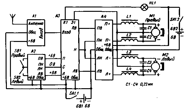
If none of the transmitter buttons is pressed, at the outputs 1,2,4 of the counter after the end of a burst of eight pulses, log.0 and at all used outputs of the decoder DD6 are also log.0. Table 1 shows the correspondence of commands to the number of burst pulses and the output signals of the system decoder. A pack of five pulses is the "Stop" command, when it is received, as already mentioned above, log.1 appears at output 5 DD6. This log.1 goes to the inputs R of triggers DD7.1 and DD7.2 and sets them to 0. We will not yet consider the role of the DD8 microcircuit and will assume that the signal does not change when passing through its elements. As a result of receiving the "Stop" command, the outputs PV, LV and H (back) will be log.0, the motors connected to the indicated outputs through amplifiers will be stopped. When the "Forward" command is given, log.1 will appear at output 6 DD6, it will set the trigger DD7.2 at the input S to state 1, the trigger DD7.1, regardless of its initial state, will be set to the state O at the input C, since at its input D log.0. As a result, log.1 will appear at the outputs of the PV and LV, log.0 will appear at the output H, both motors of the rover will rotate, ensuring the movement of the model forward. When the "Back" command is given, the trigger DD7.1 will be in state 1, DD7.2 - in state 0, the engines will ensure the movement of the model back. The specified commands are stored in the triggers of the DD7 chip and after the buttons SB5-SB7 are released. Suppose that when the model moves forward, the button SB2 "Right" is pressed. In this case, log.1 will appear at output 2 DD6, it will go to output 2 of the DD1.4 element and change log.1 at its output to log.0. As a result, the RO signal will become equal to zero, and the right engine will stop. The model will turn to the right due to the left caterpillar (the second line of Table 1). When moving backward, pressing the SB2 button will also cause the signal at the output of the DD1.4 element to change to the opposite, but now from log.0 to log.1, the right engine will also slow down and the model will also turn to the right. The model behaves similarly when the SB4 "Left" button is pressed. The commands "Right" and "Left" are not remembered, they are valid only while pressing the corresponding button. Similarly, the commands "Lights" and "Signal" (SB1 and SB3) are not remembered. When you press these buttons, the transistors VT2 and VT1 turn on, respectively. Their bases are connected to the outputs of the DD6 decoder without limiting resistors, which is permissible when the supply voltage of the K561 series microcircuits is within 3 ... 6 V. The DD8 microcircuit is used to interface the decoder of the radio control system with the board of the rover, which provides maneuver when avoiding obstacles. The use of the XOR chip ensures the controllability of the model even at those times when it performs an automatic maneuver. The complete connection diagram of the planetary rover nodes is shown in Fig.5. Here A1 is a receiver according to the diagram in Fig. 2, A2 is a board with microcircuits DD1-DD4 Fig. 211, A3 is a system decoder according to the diagram in Fig. 4, A4 are motor amplifiers. The diagram in Fig. 5 also shows the connection of the headlight lamp HL1. The author did not use the "Signal" command, the source of the sound signal can be included in the collector circuit of the transistor VT1 in the same way as the inclusion of HL1 in the collector circuit VT2.'
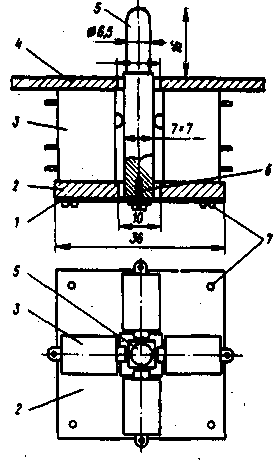
The power supply of electric motors and units A1-AZ is divided to exclude the influence of interference from engines on the electronic part of the planetary rover. The common wires of both power circuits are combined only at node A4, this should be paid attention to during installation. To eliminate the influence of interference from motors, chokes L1-L4 and capacitors C1-C4 are included in their power circuits, metal cases of motors are connected to a common wire. In the absence of node A2, voltages can be applied to the inputs P, L, C of node A3 in accordance with the instructions in Fig. 5; .8 with inputs DD 4 and DD 7.1. All nodes of the radio control system are assembled on printed circuit boards: the transmitter is on one-sided with dimensions of 60x40 mm (picture 6), receiver - on one-sided with dimensions 105x40 mm (picture 7), decoder - on double-sided with the same dimensions (picture 8). In these figures, single-sided boards are shown from the side opposite to the side where the parts are installed, the decoder board is shown from both sides. The radio control system used MLT resistors, ceramic capacitors KTM (C1 in Fig. 2), KM-5 and KM-6, electrolytic capacitors K50-6 (C4, C8, C11, C12 in Fig. 2), K50-16 (C13 in Fig. 2). The tuned resistor R6 in Fig. 2 is of type SPZ-16, its conclusions are bent at a right angle. The system uses standard chokes DM-0,2 30 μH (L2 in Fig. 2) and DM-3 12 μH (L1-L4 in Fig. 5), home-made ones with similar parameters can also be used. The quartz resonator in the transmitter is in a glass case with a diameter of 10 mm for a frequency of 27,12 or 28 ... 28,2 MHz. In the absence of a quartz resonator, the transmitter can be assembled according to any of the published schemes, retaining the burst shaper and modulator circuit according to Fig. 1. Coil L1 of the oscillatory circuit of the transmitter is wound on a frame with a diameter of 5 mm and is adjusted by a carbonyl iron core with a diameter of 4 mm and a length of 6 mm. It contains 12 turns of PELSHO-0,38 wire. The coil L1 of the receiver is wound on a frame with a diameter of 8 mm with the same wire and contains 9 turns, it is adjusted by a carbonyl iron core with a diameter of XNUMX mm. The transmitter can use the same coil as the receiver. The transmitter battery is 3336, on the model four A343 cells are used to power the engines, the electronic part is powered by four A316 cells. The receiver antenna is a bicycle spoke 300 mm long, the transmitter antenna is telescopic, consists of four knees with a total length of 480 mm. The transmitter is assembled in a plastic case with dimensions of 75x1500x30 mm, it contains a special control panel, described below. The assembly of the radio control system and its configuration must be carried out in the following sequence. It is necessary to assemble the digital part on the transmitter board, install all resistors, except R5, and transistors, but do not install a quartz resonator, L1 coil and capacitors C3-C5. By selecting resistors R1 and R2, set the pulse frequency at the DD1.2 output to 180 ... 220 Hz with a duty cycle close to 2, then check the correct generation of bursts as described above. Then you can assemble the command decoder and, by installing resistor R5 in the transmitter, connect the collector of the transistor VT1 of the transmitter to the input of the decoder. The supply voltage of both boards can use a common 4,5 V. The load of the transistor VT1 of the transmitter will be series-connected resistors R4, R6 and the base-emitter junction of the transistor VT2. The decoder should be checked as described above. Further checks can be made by first connecting the L and R inputs to the plus of the power source, the C input to a common wire. In this case, the signals at the outputs H, LV, PV when the transmitter buttons are pressed must correspond to those indicated in Table 1. After that, you can connect the nodes A3 and A4 and the engines of the model according to the scheme of Fig. 222. Inductors L1-L4 and capacitors C1-C4 should be soldered directly to the motor terminals. Next, you should check the clarity of the model control over a pair of wires connecting the transmitter and decoder boards. If everything is working properly, you should completely assemble the transmitter and receiver. After assembling the receiver, you must first adjust the resistor R6. To do this, you should "break" the super-regenerative mode of the transistor VT1 by short-circuiting the oscillatory circuit L1 C2, connect a voltmeter between the collector and emitter VT3, set the R6 slider to the minimum resistance position and, gradually increasing its resistance, set the voltage to 250 ... 300 mV on the voltmeter , while you may have to pick up the resistor R5. Shine the jumper off the circuit L1 to C2. Turning on the transmitter and receiver and gradually increasing the distance between them, you should adjust their circuits to the maximum amplitude of the signal observed with an oscilloscope or an AC voltage voltmeter at the control point KT1. Next, you should adjust the resistor R6 to obtain the correct shape of the pulses at the control point KT2 in accordance with Fig.220. Having assembled the entire model according to the scheme of Fig. 5 and making sure that the control system works normally at distances of 2 ... 3 m, it is necessary to achieve the maximum range by adjusting the resistor R6. Almost any high-frequency npn silicon transistors (KT316, KT312, KT3102, KT315 with any letter indices) can be used in the transmitter and receiver. The K561LP13 chip can be replaced by the K561YK1, if they are absent, to the detriment of noise immunity, you can exclude the comparison of sequentially incoming commands by replacing the D03-DD5 microcircuits of the command decoder with one K561IR9 chip. In the transmitter, a special remote control is used as buttons SB2, SB4, SB6, SB7, which is convenient for issuing commands with a clear directional meaning. The remote control allows you to submit simultaneously and two commands that do not exclude each other, for example, "Forward" and "Right", which, however, is not used here. Four microswitches are used as the contact system of the remote control. Figure 9 shows its design, the dimensions are indicated in relation to the PM2-1 microswitches, there are many types of microswitches with the same dimensions.
Microswitches 3 are glued to the base 2, made of textolite 2...3 mm thick. A plate 2 made of brass or tin 7...1 mm thick is attached to the base 0,2 from below with four screws 0,3 or rivets. In the center, a lever 2 made of organic glass is attached to this plate with an M5 screw with a washer. When rocking the lever 5, it presses on the rods of the microswitches 3 and switches them. If the lever is pressed diagonally, two adjacent microswitches will turn on. It is advisable to assemble the remote control in the following order. Connect plates 1 and 2 to each other, fasten lever 1 on plate 5 with a screw and washer. Glue microswitches 3 to plate 2 with epoxy glue so that microswitch rods touch lever 5. After polymerization of the glue, glue the resulting block to the console cover 4 or, to ensure maintainability, fix it in some other way, while centering the block along the square hole in the console cover. KM1-5 buttons are used as SB1 and SB1. Literature 1. S.A. Biryukov. Digital devices based on MOS integrated circuits. M. Radio and communication. 1996 Publication: N. Bolshakov, rf.atnn.ru
A New Way to Control and Manipulate Optical Signals
05.05.2024 Primium Seneca keyboard
05.05.2024 The world's tallest astronomical observatory opened
04.05.2024
▪ 3D printed objects change shape and color ▪ Fluorescent sensors will indicate organic water contaminants ▪ Experiment to simulate life on the moon ▪ Named the cause of concussion ▪ Plastic turns into edible mushrooms
▪ site section Clocks, timers, relays, load switches. Article selection ▪ article If you want to be healthy, temper yourself. Popular expression ▪ article Gluer. Job description ▪ article Consumer electronics. Miscellaneous. Directory ▪ article Riddles about clothes and shoes
Home page | Library | Articles | Website map | Site Reviews
www.diagram.com.ua |


 Leave your comment on this article: