|
|


 Arabic
 Bengali
 Chinese
 English
 French
 German
 Hebrew
 Hindi
Hindi Italian
 Japanese
 Korean
 Malay
Malay Polish
 Portuguese
 Spanish
 Turkish
 Ukrainian
 Vietnamese
|
ENCYCLOPEDIA OF RADIO ELECTRONICS AND ELECTRICAL ENGINEERING The evolution of flyback pulsed power supplies
Encyclopedia of radio electronics and electrical engineering / Power Supplies The article brought to the attention of readers is devoted to flyback switching power supplies, widely used in power supplies for televisions, computers and other electronic equipment. Such sources are also popular among radio amateurs. The article will focus on power supplies assembled on KR1033EU10 and VIPer-100A microcircuits, and their calculation using a specialized software package. PWM CONTROLLER KR1033EU10(iC3842) Switching power supplies (SMPS) became widespread in the middle of the last century already. And today, SMPSs undergo evolutionary changes almost every year. Each class of SMPS, once having conquered its niche, remains in it forever, or at least for a long time, and they develop almost independently. As powerful (150 W or more), bridge SMPSs are usually used. Reverse-running SMPSs are more often used as low-power and medium power (up to 150 W). Now the elemental base for such sources is being updated so quickly that an ordinary radio amateur and the domestic radio industry track these changes in their developments with a big delay. Integrated PWM controllers KR1033EU5 (foreign analogue - TDA4605), which were described in the article [1], have not yet been introduced into domestic household appliances, as in foreign video equipment, and especially video monitors, their new variety is already widely used - UC3842, KA3842 and UC3844 , KA3844 (domestic analogues of KR1033EU10 and KR1033EU11, respectively). Outwardly and fundamentally no different from the prototype, the relatively new PWM controllers have undergone a number of improvements. And if many radio amateurs have already met the prototype on the pages of "Radio" in [2], then the descriptions of the SMPS with PWM controllers of the UC384X series have not yet been published, except for [3], where the specified microcircuit is used in a somewhat unconventional way - as a regulator for a step-down switching voltage regulator. Let's briefly consider the main properties and differences of the KR1033EU10 (UC3842, KA3842) microcircuit, which we will continue to refer to as EU10, from KR1033EU5 (TDA4605), referred to as EU5. Both microcircuits are made in a plastic case 2101.8-1 (according to foreign terminology - DIP-8). The purpose of the EU10 pins is given in the table.
Main characteristics
The EU10 PWM controller, like the EU5, is designed to connect an n-channel insulated gate field effect transistor and basically has the same functionality. Note the first feature of EU10. The conversion frequency in the SMPS on EU5 is set automatically depending on the voltage of the mains power supply, the parameters of the microcircuit and the switching transistor, the inductance of the primary winding of the pulse transformer, the power consumption in the load, etc. Therefore, when exposed to destabilizing factors, the conversion frequency turns out to be "floating": for of any SMPS made on EU5, depending only on the load power, it can take a value from 18 kHz at maximum and up to 70 kHz at minimum load. This feature somewhat complicates the design of a transformer of such an SMPS, therefore, usually, an approximate calculation and prototyping are carried out for it first, and then, based on the test results with a real load, the necessary adjustments are made. In the EU10 microcircuit, the operating conversion frequency is set by an external frequency-setting RC circuit connected to pin 4. Since the RC circuit resistor is connected to an internal source of precision reference voltage of 5 V - pin 8, regardless of various destabilizing factors, the operating conversion frequency is rigidly fixed. On fig. 1, a shows the exponential form of the voltage Uc on the frequency-setting capacitor, corresponding to the switching pulses at the output of the PWM controller (pin 6 Uout), shown in fig. 1b.
To characterize the operating mode of the PWM controller, it is convenient to use the duty cycle of switching pulses D - this is a parameter that is the inverse of their duty cycle. The fill factor value is always less than one. However, it is not recommended to choose it more than 0,5 [3]. An additional internal counting trigger was introduced into the output circuit of the PWM controller KR1033EU11 (UC3844), which limits the duty cycle D≤0,5, but at the same time, the frequency-setting RC circuit is calculated for a double (compared to the switching pulse repetition rate) operating frequency of the internal generator. Concluding the general brief description of the UC384X series PWM controllers, we note that the UC3843 is similar to the UC3842, and the UC3845 is similar to the UC3844, but they are designed for a lower supply voltage. For them, the threshold level of the supply voltage during the transition to the "On" state for individual samples is 7,8 ... 9 V (average value 8,4 V), "Off" - 7 ... 8,2 V (average value - 7,6 V). Let us explain the concept of noise stability of a PWM controller (Fig. 1). During toff, the frequency setting capacitor charges from approximately 1,5V, which is the low threshold of the internal comparator, to a high threshold of approximately 2,75V. At this point, the PWM controller output is low. When the voltage on the capacitor Uc reaches the upper threshold level, the internal discharge circuit is turned on and the capacitor is discharged to approximately 0,75 V. The voltage at the output of the PWM controller at this moment goes into a single state. Then during the time tON. until the voltage across the capacitor reaches the lower threshold level, the switching transistor is on. It can be seen from the figure that an interference signal U with a voltage of 0,1 ... 0,5 V at the end of the charging cycle can cause premature operation of the discharge circuit and false start of the internal generator, shown by dotted lines. This property is the main disadvantage of this class of PWM controllers, but it can be significantly weakened in several ways. First, ceramic (with low inductance) capacitors with a capacity of about 7 microfarads are connected to pins 8 and 0,1 of the microcircuit. Secondly, they fulfill certain requirements for the topology of the printed circuit board and the design of the SMPS, which reduce the amplitude of interference signals, which will be explained later. Thirdly, the capacitance of the frequency-setting capacitor is chosen at least 1000 pF. And the most reliable way to completely eliminate this drawback is to synchronize the operating frequency of the PWM controller with an external source of pulsed voltage, which is described in detail in [4]. The second main difference between the EU10 is the method of monitoring the operating current in the SMPS. In EU5, the change in current in the storage winding of the transformer is simulated by an external RC circuit, and if these elements are chosen incorrectly, the switching transistor may fail. A special current control comparator is introduced in the EU10 chip, which has two inputs - inverting and non-inverting. Pin 3 is connected internally to the non-inverting comparator input. Outside, a resistive or transformer current sensor is connected to it in the source circuit of the switching transistor. As soon as the signal voltage from the current sensor exceeds the threshold value of 1 V, corresponding to the peak current value in the drain circuit of the transistor, the comparator will turn off the output amplifier of the PWM controller. For example, for a transistor with a drain current limit of 4 A, the peak value corresponding to the protection trip level is chosen to be 3,7 A. If the SMPS is overloaded, this trip will occur in each pulse, preventing damage to the switching transistor. You can adjust the level of current protection operation by changing the resistance of the resistor in the drain circuit of the transistor or by changing the transfer coefficient of the current transformer sensor. And the last, third feature of EU10, arising from the second, is the way to regulate the voltage at the output of the SMPS. Note that the principle of regulation remains the same - pulse-width control. If EU5 controls the end of the transfer of the next part of the energy by the transition of the voltage in the secondary windings through zero and then gives out such a new portion in order to maintain the voltage at the output of the auxiliary communication winding, and therefore at the load, then EU10 works a little differently. To regulate the output voltage of the SMPS, as well as to neutralize the negative influence of destabilizing factors, the input of the error signal amplifier - output 2, is used, to which an additional auxiliary winding of the transformer is connected, thereby forming an external feedback loop, called the primary control loop. The amplifier monitors the disturbing effect of destabilizing factors and corrects the parameters of the switching pulses so that the voltage at the output of the communication winding and at the load remains constant. The frequency and phase properties of the transfer characteristic of the error signal amplifier, which determine its stability, are regulated by an external RC circuit connected to pin 1, which is internally connected to the output of this amplifier. Thanks to this architecture of the microcircuit, the developers provided for the possibility of using pin 1 for remote or emergency shutdown of the SMPS (transfer to STANDBY MODE - standby mode), closing it to a common wire using an external transistor. If an optoelectronic sensor is connected to this output and is electrically connected to the output, a second output voltage control loop is obtained, which improves the stabilizing properties of the SMPS and, in addition, makes it possible to implement a "soft" start of the SMPS. Stabilization of the output voltage of the SMPS occurs as follows. The output of the error signal amplifier inside the microcircuit is connected through matching circuits to the inverting input of the current control comparator. A current sensor is connected to the non-inverting input of the comparator. In the current comparator, from the moment of the beginning of each switching pulse, these two signals are compared. If the signals coincide, each switching pulse will stop at the moment when the current in the storage winding reaches the required peak value. In normal mode, this will happen much earlier than the peak current reaches the limit value of the drain current of the switching transistor. In turn, the peak current determines the operating power of the transformer. The energy stored in the storage winding of a transformer with inductance L is determined by the equation W=LIP2/2, and if the accumulation of energy is stopped at this moment, when the linearly increasing current in the winding reaches the required peak value IP, the secondary power circuits will receive the necessary portion of energy. Moreover, if at a constant voltage of the mains power supply U0 we compare two versions of the converter, which differ, for example, by a factor of two in the conversion frequency, the inductance of the storage winding should also differ by a factor of two. This is necessary in order to change the rate of rise of the sawtooth current, determined by the ratio U0 /L. Therefore, for example, if the current in the winding at a conversion frequency of 100 kHz at the time of the switching pulse reaches a peak value after 2 μs, then at a frequency of 50 kHz, due to a doubling of the inductance at the same voltage U0, after 4 μs. The power for both options remains the same, since in the expression characterizing it P=W/T (T=1/f is the period of the conversion frequency), both the numerator and the denominator will change proportionally. But the dimensions of the transformer magnetic circuit for these options will differ significantly: the higher the frequency, the smaller the required magnetic circuit for the same power. Similarly, with a constant inductance L and a changing voltage U0, the time interval tON will vary. during which energy is accumulated in the primary winding of the transformer, since it is inversely proportional to the ratio U0 /L. Thus, the stored energy in each pulse remains constant and does not depend on destabilizing factors. Radio amateurs who wish to study in more detail the block diagram, functional description and features of the EU10 chip device can refer to the reference book [4]. POWER SUPPLY ON CHIP KR1033EU10 Scheme of the proposed simplest version of the SMPS. the basis of which is the PWM controller KR1033EU10 (UC3842, KA3842), shown in fig. 2.
Main parameters of SMPS
The mains voltage source, as well as the low-frequency and high-frequency mains filter, are made similarly to the prototype [2] and have no special features, except that the element that limits the inrush current when the SMPS is turned on is a thermistor RK1 with a negative TCS. When turned on, its resistance is maximum, and then as it heats up under the influence of the current consumed by the device, it decreases. This helps to protect the network diode bridge VD1 from damage in the starting mode. True, with a quick re-start, the effectiveness of such protection is low. The voltage divider R1 - R3 in the error signal amplifier circuit provides adjustment and stabilization of the output voltage of the SMPS using the primary control loop. Resistor R6 provides power to the microcircuit in the starting mode, when the current consumed by it does not exceed 1 mA. After switching on the SMPS, the rectified mains voltage through the limiting resistor R6 is supplied to the filter capacitor C11 in the power supply circuit of the microcircuit. When the voltage on the capacitor reaches the threshold level for the transition of the microcircuit to the "on" state (typical value - 16 V), the comparator is triggered and power is supplied to all elements of the PWM controller, after which the internal reference voltage source is turned on, then the switching pulse generator and the output amplifier. The SMPS switches from starting to operating mode, providing power to the microcircuit from the auxiliary winding of the transformer connection through the VD5 diode. The current consumed by the microcircuit increases to 11 ... 17 mA. If the mains voltage drops, the output voltage of the SMPS and the supply voltage of the microcircuit will gradually decrease. The rate of decrease in the output voltage is hundreds of times less than the input voltage due to stabilization, however, there will come a moment when the microcircuit supply voltage reaches the threshold level for switching to the "off" state (typical value is 10 V). At this moment, the comparator will work and the power from all elements of the controller will turn off. The difference (6 V) between the threshold levels for switching on and off the microcircuit (supply voltage hysteresis) is necessary to prevent random switching of power circuits in the starting mode. The repetition rate of switching pulses (the operating frequency of conversion to the SMPS) is determined by the parameters of the R5C8 circuit. In order for the conversion frequency to correspond to the calculated value f = 30 kHz, it may be necessary to select the values of the frequency-setting elements. How to determine the required values of the frequency setting elements for a different operating frequency will be discussed later. Particular attention in the design of the described variant of the SMPS is given to ensuring its noise stability. To a large extent, the overall stability of the controller error signal amplifier, and hence the SMPS, is determined by the parameters of the R4C5 compensation circuit. The following elements serve the same purpose: the VD2 diode, which eliminates surges that are negative relative to the common power wire of the voltage microcircuit during the fall of switching impulses; zener diode VD3. limiting "sharp" surges of positive voltage at the fronts of switching pulses; inductor L2 and current-limiting resistor R7, which prevent self-excitation of the switching transistor at high frequency. The ceramic capacitors C9 and C10, connected directly to pins 7 and 8 of the microcircuit, significantly increase the stability of the amplifier. On the current sensor - resistor R11 - sawtooth voltage pulses are formed for control and protection circuits, the peak value of which depends on the drain current of the switching transistor. The signal amplitude becomes equal to 1 V at a drain current of 3,7 A. This ensures reliable protection of the transistor from damage. The oxide capacitor C13, connected in parallel with the resistor, significantly attenuates switching noise, preventing false operation of the current control comparator. Capacitor C7 serves the same purpose. Capacitor C6 corrects the slope of the sawtooth voltage at pins 3 and 4 of the microcircuit, significantly attenuating high-frequency noise, which also ensures the required stability of the controller. No less effective measures are required to reduce the amplitude of interference generated in the SMPS. A very important role in this is given to the electrostatic screen installed on the pulse transformer. Strong interference is also emitted by a heat sink, on which a switching transistor is installed, if the heat sink is not connected to a common wire, and the transistor is not isolated from it with a mica plate. Significant interference generates pulsed currents flowing in the conductors connected to the drain of the switching transistor and to the output winding. In order to weaken them in the described SMPS, the transistor is connected to the transformer with a short piece of coaxial cable, and the printed conductor connecting the rectifier diode and the output winding is chosen to be of minimum length and large cross section. It is quite obvious that a considerable contribution to the creation of interference is made by switching processes that occur at the moment the transistor is turned on and off. The presence of the interelectrode capacitance drain-source in the field-effect transistor, as well as the distributed capacitance and leakage inductance in the windings of the transformer leads, at the moment the transistor is turned off, to the appearance of an “acute” surge of significant voltage on its drain, and then an exponentially damped high-frequency signal. The filling frequency of this signal, if no special measures are taken, is determined by the leakage inductance of the transformer and the interelectrode capacitance of the transistor. The damper circuit VD4R10C12, connected in parallel with the storage winding of the transformer, suppresses free oscillations in this signal and "binds" the voltage surge to the mains power supply. Usually, in flyback converters, an additional capacitor with or without a series-parallel connected resistor and diode is connected relative to the common wire (source) to the drain of the switching transistor. These elements not only effectively suppress switching processes, but also help to reduce the rate of voltage rise at the drain of the transistor at the moment it is turned off, thereby preventing dangerous dissipation of instantaneous power on the transistor and transferring the combination of maximum operating current and maximum operating voltage to the region of safe operating modes. In the described SMPS, this function is successfully performed by the inductor L3. The rectified output voltage is fed to the load through a U-shaped filter, due to which the output voltage ripple is reduced to the required level. Capacitor C17 connects the output and input circuits of the SMPS at high frequency, effectively attenuating the generated interference and significantly improving the electromagnetic compatibility of the SMPS with devices connected to the power circuits. A drawing of the printed circuit board of the SMPS is shown in fig. 3. It is made of one-sided foiled fiberglass 1,5 mm thick and basically repeats the design of the prototype [2]. The exception is the large areas left on the board with continuous metallization, which contribute to an increase in the noise immunity of the device.
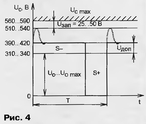
Non-deficient parts and elements are used in the device. Capacitor C1 - K73-17 for a rated voltage of 630 V, C2, C3 - K15-5, C12 and C17 - K78-2 or K15-5 for a rated voltage of at least 1000 V. Oxide capacitor C4 - K50-32. It is permissible to replace it with domestic K50-35B or an imported analogue. For capacitors C9 and STO - KM-5 - the conclusions are shortened to the optimum minimum and soldered directly to the conclusions 5,7 and 8 of the microcircuit from the side of the printed conductors. Oxide capacitor C13 - K53-14 or another tantalum capacitor C11 - K50-35. Oxide capacitors C14 - C16 - imported. You can use domestic ones, but they have slightly larger sizes. All other capacitors - any ceramic for a rated voltage of at least 50 V. The imported SCK105 thermistor, where the first three alphabetic characters indicate the series, the fourth and fifth numeric characters indicate the nominal resistance in ohms at a temperature of 25 ° C, and the last digit indicates the maximum operating current in amperes, it is permissible to replace domestic with similar parameters. All resistors are OMLT, with the exception of the imported resistor R11, which approximately corresponds in size to the domestic OMLT-1. Trimmer resistor R2 - SPZ-38b. We will replace the KTs405A (VD1) rectifier bridge with separate diodes with a permissible reverse voltage of at least 400 V and a current of at least 1 A. Diode D310 (VD2) with a permissible forward current of 0,5 A and a reverse voltage of 20 V can be replaced with a modern one with a Schottky barrier, at which the direct voltage drop at maximum current does not exceed 0,5 V. The zener diode (VD3) can be replaced by any other low-power one with a stabilization voltage of 16 ... 18 V. The pulse diode in place VD4 (KD257D) must be designed for an operating frequency of at least 50 kHz , the maximum reverse voltage is 1000 V and the maximum current is 3 A. We will replace the KD220B (VD5) diode with a KD220A or another with similar parameters. The rectifier diode KD213B (VD6) with an operating frequency of up to 100 kHz can withstand a reverse voltage of 200 V and a maximum current of 10 A. Parallel connection of such diodes, designed for a lower current, without current-leveling resistors is permissible. It is also possible to use modern diodes. We will replace the KP707V2 transistor with imported analogues with a maximum drain-source voltage of at least 700 V and a permissible drain current of at least 4 A. Install it on a heat sink with an effective cooling area of 100 ... 200 cm2 through a mica plate coated on both sides with heat-conducting paste KPT- 8. The output of the transistor drain from the side of the printed conductors of the board is connected to the transformer with a short piece of coaxial cable with an outer diameter of about 5 mm, after passing the central core through the ferrite tube. On fig. 3 conditionally shows the start and end points for connecting the inductor L3, but the image of the cable segment is not shown. To eliminate additional interference, the cable braid should be connected to a common wire in strictly defined places: on the one hand, in the immediate vicinity of the connection point of the VD4 diode and terminal 3 of the transformer, on the other, at the common zero potential point R11C13. The ferrite tube is glued through an insulating gasket to the board from the side of the printed conductors under the elements R11, C13. It is permissible to replace the industrial choke of the line filter L1 with a home-made one. It is wound in two conductors MGTF 0,35 on a ferrite ring radio tape recorder 1500NM-2000NM with an outer diameter of about 20 mm until filled. Inductors L2 and L3 are pieces of tubes 5 ... 7 and 10 ... 12 mm long, respectively, made of high-frequency ferrite used in DM-1,0 chokes, etc. To obtain the inductance values indicated in the diagram, for the L2 choke, one a turn of PEVT wire 0,41, and for L3 - two turns. In the author's version, similar imported products were used, while it took one turn (through passage) for each throttle. Choke L4 is wound on a segment of a rod with a diameter of 10 and a length of 35 ... 40 mm from 400NN ferrite. Its winding contains 30 turns of PEV-2 1,5 wire. The magnetic circuit of the transformer T1 is assembled from two halves of Sh12x20x21 ferrite M3000NMS2, used in television power supplies for televisions 3 (4) USCT, etc., with a non-magnetic gap on the central rod of 2,4 mm. The windings are wound on a standard frame with contact leads, the numbering of which corresponds to that shown in the diagram. They are performed as follows. First, the first section of the primary winding is wound - 26 turns of PEVT 0,41 into two wires. It is isolated with two layers of 0,05 mm thick varnished fabric. An output winding of 25 turns of PEV-2 1,5 wire is wound over the insulation. In this case, the conclusions 10, 12 and 14 present on the frame are removed, and the winding wire is used as the conclusions, passing it through the slot between the conclusions 10 and 12, 12 and 14, respectively. In the diagram, the pin numbers are conventionally designated 10a and 12a. Then two layers of insulation are laid and a second section of the primary winding is wound on top of it, containing 44 turns. The last winding is an auxiliary communication winding of 12 turns of PEVT wire with a diameter of 0,15 ... 0,21 mm, evenly distributing it over the entire width of the frame and covering it with another layer of insulation from above. After gluing the ferrite plates of the transformer, the windings, together with the magnetic circuit, are covered with an electrostatic screen from a single layer of copper foil. The number of turns in the windings is determined by the magnetic circuit and the non-magnetic gap, therefore, for another magnetic circuit, they should be recalculated. The SMPS is connected to the network with a two-wire cable, the break of which includes a PKn41 switch or a TV2-1 toggle switch, as well as a 2 A fuse. If during the manufacture of the transformer the phasing of the windings is not violated and serviceable parts are used, the adjustment of the device is reduced to setting the output voltage with a tuning resistor R2. The use of elements of the R5C8 frequency setting circuit without their preliminary selection may lead to a slight deviation of the operating frequency from the calculated value. The type and ratings of most of the elements used in the SMPS were determined in accordance with the results of computer-aided design, which will be discussed later. DESIGN FEATURES OF REVERSE SMPS It is possible that the described IIP will completely satisfy one of the radio amateurs, and he will decide to repeat it without changing anything. But the probability of such an event is very, very small: depending on the scope of amateur radio interests, and they are always multifaceted, you may need a source whose parameters will differ significantly from those given. Therefore, in most practical cases, it will be necessary to modify the described device and make certain changes to it. The group of companies STMicroelectronics, producing radio-electronic components, has developed and sells on the world market, including the Russian market, a line of microcircuits under the trade name VIPer. Without going into the specifics of the abbreviation used, we only note that this product is an integral version of the main fragment of the SMPS, including a switching transistor and a PWM controller. As conceived by the developers, such microcircuits should greatly facilitate the work of designers and operators of the SMPS. Some (2...4 times - depending on the selected chip) increase in the cost of the element base of the VIPer-switched SMPS, in comparison with its discrete version, is fully offset by the capabilities of automated design, as well as quick recovery by simply replacing the chip in the event of a malfunction. . For automated design of SMPS based on VIPer microcircuits, the same company has developed a freely distributed software package VIPer Design Software. The latest version of the program (v2.12) with a capacity of 4 MB can be downloaded from the developer's website . This software package, hereinafter referred to as DS (Design Software), can be successfully used to design the described SMPS option based on the UC3842 PWM controller. A user-friendly interface allows you to complete such a complex task in a matter of minutes. Before using DS, let's clarify some design features related to the choice of elements and setting the operating conversion frequency in the SMPS. It must be remembered that in pulse flyback transformers, the magnetic circuit is always made with a non-magnetic gap on the central rod (core). We are talking about transformers with Ш-shaped plates, as well as modern KB (foreign analogue of RM) magnetic cores [5, 6]. Let us also pay attention to the preference for using ferrite for pulse transformers, for example, the M3000NMS-2 brand, in the name of which there is a symbol C. This is a sign of the ability of a magnetic wire made of this material to work in strong magnetic fields, which is due, unlike the others, to negative temperature coefficient of specific losses. Despite the decrease in efficiency and the deterioration of the electromagnetic compatibility of the transformer with other elements, it is impossible to refuse a non-magnetic gap. Firstly, in strong magnetic fields, the gap prevents saturation of the magnetic circuit, and secondly, with the correct choice of the operating mode of the switching transistor, the presence of a gap prevents an excessive increase in the amplitude value of the current pulses in its drain circuit. Therefore, we have to put up with losses and take into account the fact that the intensity of noise radiation associated with the fundamental and higher harmonics of the operating frequency of the conversion increases relatively quickly after 100 kHz. Of course, there are magnetic materials in which the domains are separated from each other by a non-magnetic substance (for example, from a magnetodielectric based on molybdenum permalloy grades MP-60, MP-140, MP-160, MP-250, etc.), in which the gap seems to be distributed over the entire working volume of the magnetic circuit and therefore, in principle, it is possible to use solid magnetic circuits without a gap. The second source of losses in the SMPS is the increasing resistance of the winding conductors due to a decrease in the field penetration depth at higher frequencies. Therefore, to reduce the losses caused by this phenomenon, it is desirable to wind the winding from several parallel conductors, the cross-sectional area of which is equivalent to the original one, but the side surface along the perimeter of the conductor cross-section is several times larger. More precisely, the increase in the lateral surface in this case is proportional to the square root of the number of parallel conductors. The third source of losses is associated with the magnetization reversal of the magnetic circuit. And, finally, the last, fourth source of losses is due to the need to use various resistive-capacitor circuits that suppress transient switching processes, and the limited speed of the radio elements used in the SMPS - oxide capacitors, a field-effect transistor, rectifier diodes. The non-sinusoidal (impulse) voltage on these elements and the large current amplitude (up to several amperes) lead to a significant specific weight of losses in them. All these losses must be taken into account when designing an SMPS using DS. Since losses in the transformer lead to heating of its windings and magnetic circuit, one of the criteria is used to evaluate them: either the allowable temperature rise of the transformer without its forced cooling, which is usually chosen within 30 ... 50 ° C, or the specific weight of losses is assumed to be 1 ...5% of the transformer capacity. The overall performance of the SMPS is evaluated based on the efficiency. In the best case, its value can reach 92...95%, in the worst - 60...65%. SELECTION OF THE SWITCHING TRANSISTOR AND RECTIFIER DIODES The switching transistor without any calculations can be selected with a multiple margin. And it is possible to solve this problem more rationally. How to determine the parameters that the switching transistor must correspond to, depending on the technical characteristics of the designed SMPS? Unfortunately, the DS package does not directly answer the question posed. Therefore, we first consider the shape of the pulsed voltage at the drain of the transistor Uc (Fig. 4).
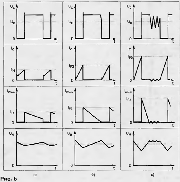
In accordance with the initial data, at a nominal voltage of 220 V at the output of the mains rectifier, without taking into account the voltage drop across the rectifier diodes and thermistor, we obtain [7] U0 = 220√2 \u310d 80 V. In addition, at the drain of the transistor there is some additional to the rectified mains voltage Uadm. In foreign literature and in DS it is called UR (reflected - reflected, induced). As the results of the trial design of several variants of pulse transformers show, its value always turns out to be very close to the default value of XNUMX V proposed in DS. Let's show how to determine the real value of the additional voltage. The voltage across the inductor is directly proportional to the rate of change of current in it: U = LΔI/Δt or U Δt = L ΔI. Since the current changes with the transistor on and off for the steady process are the same, the areas of the rectangles marked S+ and S- in Fig. 4. Calculating their areas, we get the equation Uo·D·T = Uadd(1-D)T or after transformations Uadd = Uo·D /(1-D). On the other hand, in accordance with the geometric interpretation of the energy transfer process, the output voltage on the secondary winding is the transformed additional voltage on the primary winding: Uadd \uXNUMXd k Uout, where k \uXNUMXd wl / wout - the transformation ratio (wl, wout - the number of turns of the primary and output windings, respectively). Strictly speaking, the assumption that each portion of energy taken from the network in the first cycle is transferred without a trace to the load in the second cycle, as shown in Fig. 4 as a solid line, and at the same time the transmission ends exactly at the moment the transistor is turned on, is to some extent conditional. In reality, SMPSs can operate in two modes: continuous magnetic flux mode and discontinuous flux mode. In practice, this means that if by the time the switching transistor is turned on, the current in the windings is zero, then this mode corresponds to the intermittent flow mode. Otherwise, the continuous flow mode takes place. On fig. 5 shows diagrams of voltage and current in the elements of the SMPS: Uc - voltage at the drain of the transistor; lc - drain current of the switching transistor; lw out - current in the secondary winding; UH - load voltage.
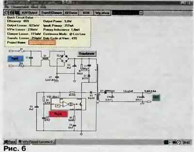
The continuous current mode corresponds to fig. 5, a. Its main feature is that the transistor turns on at a certain drain current. The advantage of the mode is the smallest peak current in the SMPS elements compared to other modes and the smallest output voltage ripple. If, by reducing the mains voltage to a minimum, it is possible to increase the pulse duty cycle by more than 50%, DS warns the user to make adjustments to the calculations. This is due to the peculiarities of the magnetization of the magnetic circuit in a single-cycle pulsed mode and the possibility of increasing the amplitude of the transistor drain current over the allowable limit. The intermittent current mode is shown in fig. 5, c. After the energy transfer process is completed, the diode closes. In the windings, damped free oscillations arise in the fall of the impulse voltage. This mode is characterized by the highest current amplitude in the SMPS elements and the maximum output voltage ripple. The optimal one is the transitional mode between the two named, shown in Fig. 5 B. The DS program allows you to control the amplitude, shape of the current and voltage on the transistor, as well as determine the operating mode of the designed SMPS and the value of the pulse duty cycle at any possible mains voltage. A significant addition to the voltage acting on the drain of the transistor is made by leakage inductance (in DS it is designated Leakage Inductance). It is directly related to the stray fields in the transformer. During the action of switching pulses, when the transistor is open, energy is accumulated not only in the storage winding, but also in the leakage inductance. When the transistor is turned off, this energy leads to an additional voltage surge on its drain, shown in Fig. 4 dotted line. To limit it, damper circuits are used. In the DS program, you can choose either a resistive-capacitor circuit (RC Clamp), or a limiting zener diode (Transil Clamp). The calculation of the leakage inductance and the associated voltage surge is a very difficult task, since it is necessary to take into account the inductance and interturn dynamic capacitance of the windings, the non-magnetic gap in the transformer magnetic circuit, the sectioning of the windings, the design parameters of their execution, and many other factors. The DS program uses some average value of leakage inductance, which, if necessary, can be changed by the user forcibly. The level of voltage surge limitation in each specific case of SMPS design can be controlled in the Waveform window (oscillogram) and taken into account when choosing a transistor according to the maximum allowable drain-source voltage. Choosing a rectifier diode in DS is not difficult. The OUT window provides the necessary information about its parameters: forward and reverse current, forward drop and the maximum allowable reverse voltage. AUTOMATED DESIGN OF REVERSE SMPS So, turn on the computer and run the DS program. A splash screen appears on the monitor screen for a few seconds, and then a window opens (Fig. 6). By default, the program loads the "preparation" project under the name "Default.vpa".
Move the mouse cursor to the blue on-screen button Input (input), and a pop-up hint appears on the monitor screen: Edition of AC Line Parameters (editing AC line parameters). We press the button. The Input Parameters window appears on the monitor screen, shown in fig. 7.
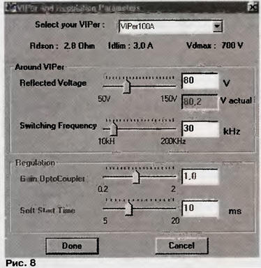
In the Line Frequency section, set 50 Hz, in the AC Input Range section (input AC voltage interval) using the slider, or after placing the cursor in the appropriate window - by typing from the keyboard, - set Minimum Voltage (minimum voltage) and Maximum Voltage (maximum voltage), the first - with an accuracy of 5 V, the second -10 V. You can set any of the voltages from the keyboard with an accuracy of 1 V. For most devices, the allowable change in mains voltage is considered to be -10 ... + 5% of the nominal or after rounding in the direction of increasing the interval - 195 ... 240 V. You can set the interval and a little wider, but in any case, you should not leave it set by default, because the larger it is, the more stringent the requirements are for the element base used. Then, in the same window, go to the Input Ripple section (amplitude of the input voltage ripple) and set its required value. The capacitance of the filter capacitor of the mains rectifier and the amplitude of the output voltage ripple will depend on this parameter, which in turn also depend on the load current and on the capacitance of the output filter capacitor. The acceptable ripple value is 10 ... 30 V. Set 30 V, and click on the Done button - done (you can cancel the changes made if necessary with the Cancel button). The Input Parameters window will automatically close and the system will make some adjustments: for example, the capacitance of the mains rectifier filter capacitor will change. At the next design stage, we proceed to setting the operating conversion frequency and pre-selecting the switching transistor, for which we press the VIPer button. In the appeared window VIPer and Regulation Parameters (VIPer and regulation parameters) (Fig. 8) in the Select your VIPer window (select VIPer), we call the drop-down list of products and select VIPer 100A. Now, just below its name, the main parameters will be displayed: Rdson: 2,8 Ohm (resistance of the drain-source section in the on state); Idlim: 3,0 A (drain current limit); Vdmax: 700 V (maximum drain voltage). In the Around VIPer section ("around" VIPer), the value of Reflected Voltage (reflected voltage) is left set by the system, Swiching freguency (switching frequency) is set equal to 30 kHz. This will reduce losses and avoid scarce parts, although to minimize the size of the transformer it is better to use a higher frequency - up to 100 kHz. The Regulation section remains inactive and is not editable. This can be done only after the introduction of the secondary control loop. Click on the Done button (done). The window will automatically close.
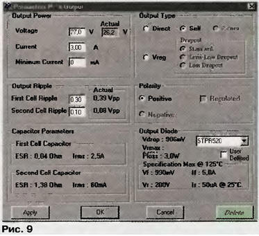
After that, go to the green button Out (exit). In the Parameters Main Output window that opens (parameters of the main output voltage source) (Fig. 9), we proceed to editing the Output Power section: in the Voltage window, set 27 V; in the window Current (current) we type 3 A; in the window Minimum Current (minimum current) we leave the 0 mA set by the program, which implies the possibility of working in idle mode.
Next, edit the Output Type section (output filter). You can leave the default Self U-shaped LC filter. If you select Direct (filter - capacitor connected in parallel with the load), a very large capacitor may be required. If Vreg (voltage regulator) is selected, an additional integrated linear voltage regulator will be installed at the output. In this case, you must specify the Dropout value (voltage drop across the stabilizer). There is a choice of Standard (standard), Low Dropout (low) and Semi-Low Dropout (medium). Leave the output filter as Self. Let's move on to editing the value of the output voltage ripple - the Output Ripple section: in the First Cell Ripple (ripple in the first stage) window, set 0,3 V, Second Cell Ripple (ripple in the second stage) - 0,1 V. After all the above manipulations, click on the Apply button. The program will immediately calculate the parameters of the output circuit elements and present the results of calculations for the rectifier diode: Vdrop: 906 mV - forward voltage drop, Vrmax: 150 V - maximum reverse voltage part of the pixels of the specified element), Ploss: 3 W - losses on the diode; Specification Max@125 °С - parameters of the STPR520 diode at the specified temperature: Vf: 990 mV - forward voltage drop, If: 5 A - admissible forward current, Vr: 200 V - limiting reverse voltage; Ir: 50 uA @ 25 °C is the maximum reverse current at the specified temperature. According to the reference book, we select a close domestic analogue of KD213B. It should be noted that due to the shape of the pulsed voltage, which is very different from the meander, the rectifier diode, participating in the formation of a relatively low voltage of 27 V, experiences a significantly higher reverse voltage - about 150 V - and take this fact into account when choice of diodes. After completing this design stage, click on the OK button of the open Parameters Main Output window, after which it closes. And the last design stage is connected with editing the parameters of the pulse transformer. Click on the gray Transformer button, after which the Transformer Design window will open (transformer design), shown in fig. 10.
The window contains two main sections: Transformer Parameters (transformer parameters) and Transformer Outlook (transformer output), the contents of which correspond to the transformer, the standard size of which is indicated in the Core Size section (core size). The program uses the smallest possible core size, according to the default loss criterion Temperature Increase in the Core Selection Criteria section. Opposite this criterion, a checkbox is set, in the same line with which its values are indicated: Target 40°С (permissible) and Actual 34,8°С (actual). At the same time, the values of the secondary criterion Dissipated Power (dissipated power) correspond to Target 2%, Actual 2,2%. The latter, as exceeding the established norm, is displayed in the window on a red background. If you select the second criterion as the main one (reset the checkbox opposite its name), and then click the Apply button, the transformer parameters will immediately change In the Geometry window of the Core Size section, the dimensions of each plate are given in the following order: width/height/thickness E36/18/11 E serie (geometry for the E series - a foreign analogue of W-shaped plates). Almost the same dimensions have a domestic counterpart W 10x10. If you use it, you can skip to the next section. If such a magnetic circuit is not available, but there is Ш12x20x21 made of M3000NMS2 ferrite, used in power supplies for TVs 3 (4) USCT and others, it is necessary to recalculate the parameters of the transformer. To do this, in the Core Size section, check the box in the Fixed window and click on the Edit button, after which the Core Size window will appear (Fig. 11).
We leave the shape of the magnetic circuit E serie unchanged (if necessary, in the same window, you can select another magnetic circuit from the proposed list, for example, the RM10 series). Next, in the Geometry window, we select a standard size close to the existing E42/21/20. Click on the OK button, after which the Core Size window will close. Now in the Core Size section, you can read the parameters of the selected magnetic circuit: Ae 236 mm2 (cross-sectional area); Le 98 mm (average length of the magnetic line); Lm 85 mm (average coil length); W 200 mm2 (window cross-sectional area); Ve 23100 mm3 (volume of the magnetic core). Please note: after increasing the size, the red banner corresponding to the non-main criterion Dissipated Power disappeared - earlier its Actual value of 2,2% exceeded the required one, but now it has returned to normal and amounts to 1,4%. Let's move on to the content of the Core Material section. By default, the program offers: Type N27, Supplier SIEMENS (ferrite grade N27 from SIEMENS). Comparing its parameters with the characteristics of domestic M3000NMS2 ferrites given in the handbook [8], we note their good agreement. If you have to use some other ferrite, you should check the box in the User Defined window (defined by the user) and click on the Edit button, after which the Transformer Core Material window will appear (transformer magnetic core material), shown in Fig. 12.
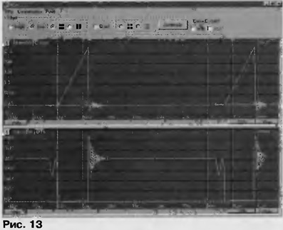
It has the ability to select the manufacturer and brand of ferrite, the parameters of which are displayed in the same window. It is important to note that whichever ferrite you choose, the value of the Primary Inductance parameter (see Fig. 10) remains unchanged. Refer to the Transformer Outlook section (transformer output parameters) for information about transformer windings. Now they can be rewritten (or printed on a printer, there is such an opportunity) and proceed to practical implementation. Some calculation errors, like any other destabilizing factor, will be leveled by the automatic control units of the PWM controller, but this will reduce the stability margin of the SMPS for other disturbing influences. Therefore, it is still better not to rush and correct the results of computer-aided design, bringing them as close as possible to the real ones. CORRECTION OF DESIGN RESULTS Let's turn again to the Transformer Design window, shown in fig. ten. In the section Wire Selection Parallel Conductors (selection of parallel conductors in the winding), leave the default checkbox set by the program on the item Single Wire (single conductor), which will correspond to the use of single conductors in the winding. If you select the item //Wires (parallel conductors) and in the corresponding window correct the 10 conductors installed by the system for another expected number, depending on the operating frequency, the program will recalculate the transformer windings with new initial values. It is possible to use conductors of the same diameter for all windings. To do this, just put a "tick" in the Single Diameter box and press the Apply button. We will restrict ourselves to the use of single conductors of various diameters. Now in the Transformer Outlook section you can read reference information on all windings: Input AWG20 75T 1W (primary - wire No. 20 according to the AWG standard, 75 turns of single wire), Auxiliary AWG42 13T 1W (auxiliary - wire No. 42, 13 turns), Out AWG 13 26T 1W (output - wire No. 13, 26 turns). To find out the wire diameter in millimeters, go to the AWG Details section and click on one of the three colored buttons, the color of which matches the color of the windings. In the heading AWG Details, the corresponding name of the winding appears, and below - its geometric and electrical parameters. For example, for auxiliary winding (Aux) Ø64 um Iso 76 um; Rdc=6,9R; Rac \u6,9d 64 R (diameter - 0,064 microns \u0,076d 6,9 mm, with insulation - 6,9 mm; DC resistance - XNUMX Ohms; AC resistance - XNUMX Ohms). In the section Transformer Usage (transformer use) the main norms are given, characterizing some reserves that must be provided when designing a transformer. These include Window Factor Utilization (window section fill factor), which by default should not exceed 80%, and Bsat Margin (maximum induction margin in the magnetic circuit) relative to induction in Bsat 380 mT saturation mode - at least 25%. Flux Density 116 mT is calculated to be only about 30% of the maximum possible, i.e. the margin is 70% and the margin requirement is met. Such a low magnetic induction is due to the non-magnetic Air Gap indicated here, equal to 2,28 mm. In accordance with the design algorithm, the program calculated that the inductance of the Primary Inductance in this case should be 0,73 mH. But if we take a critical approach to the design results, it is necessary to take into account the error in the calculations in advance. Reference books for ferrite products indicate that their electromagnetic parameters may differ from the given values by ± 25%. Therefore, it is better not to rely on chance and not to overload the complex of destabilizing factors with additional disturbing influences, but to correct the design results. This applies, first of all, to the inductance of the primary winding of the transformer. Since when developing an SMPS, a radio amateur may have a magnetic circuit with a non-magnetic gap that differs from the calculated one. This circumstance also indicates the need to take into account the real inductance of the primary winding. Known mathematical formulas do not allow to calculate the inductance of the primary winding with high accuracy, since they do not take into account the strong influence of the non-magnetic gap on the effective magnetic permeability of the magnetic circuit material. Therefore, it is easiest to wind a test winding with the number of turns wprobes on the available magnetic circuit. measure its inductance Lprobe, and then calculate the number of turns w required for a given inductance L: w = wprobe√ L/L samples. Obviously, the inductance of the winding depends very little on the diameter of the conductor. It may happen that the radio amateur did not have the range of winding wires required by the system, but there is a set of wires of a different diameter that can be used to make a transformer. For example, for the primary winding, the program recommends using a wire with a diameter of 0,812 mm. Moreover, at a conversion frequency of 30 kHz, you will not be able to "force" the program to switch to parallel conductors. Nevertheless, in most pulse transformers of television power supplies, the windings are made of several parallel conductors. Let's perform this operation outside the computer-aided design system. From the condition of equality of the side surface, equating the circumference of a single and parallel conductors, we determine their diameter: d2 \u1d d2 / 0,41 -XNUMX mm. The inductance of the primary winding of the transformer, containing 26 turns of two PEV-2 0,41 conductors, wound on a magnetic circuit made of transformer plates Ш12x20x21 with a non-magnetic gap on the central rod of 2,4 mm, turned out to be 103 μH. To obtain the required inductance of 730 µH, the winding should consist of approximately 70 turns. Proportionately adjust the remaining windings recommended by the program: w2 = (70/75) 13 -12 turns; wvyx \u70d (75/26) 24 - XNUMX turns. The real inductance of the primary winding of a transformer manufactured in accordance with the given parameters is approximately equal to 770 μH, which is in good agreement with the calculation. For the output winding, the program recommends using a wire with a diameter of 1,8 mm, while the resistance of the winding for direct current will be 25 mΩ, and for alternating current - 38 mΩ. Unfortunately, the author did not have the required wire at his disposal, so he had to be replaced with an existing one of a different diameter - 1,5 mm. The inevitable increase in the resistance of the winding and the corresponding decrease in the output voltage will have to be compensated by an increase in the number of turns 25. A significant margin of the calculated temperature rise of the transformer (15,5 ° C versus the permissible 40 ° C) gives the right to hope for the validity of such a correction. Completing the calculation of the transformer, we determine the additional voltage Udop = (70/25) 27 = 75,6 V, and taking into account the efficiency - 81,6 V, which is very close to the one set by the program, and therefore to the VIPer window (see Fig. 8 ) may not be returned. We turn to the choice of a switching transistor. On the DS toolbar, click on the Waveform button (oscillogram), after which the window shown in Fig. 13, in which up to four different parameters of the SMPS can be observed simultaneously by choice.
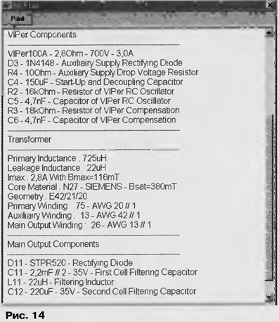
We leave the two windows offered by the system for viewing oscillograms, and in the first window we will display the dependence Idrain = f(Vin)@Pmax (dependence of the drain current on the input voltage at maximum power consumption), and in the second - Vdrain = f(Vin)@Pmax (dependence drain voltage versus input voltage at maximum power consumption). By changing the input voltage using the slider on the scroll bar, you can explore the nature of the transformation of these parameters. From these diagrams, the following conclusions can be drawn: for all permissible changes in the mains voltage and load parameters, the designed SMPS operates in the intermittent current mode - this is additionally indicated by the inscription in the upper right corner of the windows with oscillograms; the amplitude of the drain current of the switching transistor at the maximum mains voltage is 2,7 A; at a minimum voltage, the current amplitude remains the same, and the duty cycle of the switching pulses increases from 0,18 to 0,24; the maximum voltage at the drain of the transistor (at the maximum mains voltage) reaches 640 V. The results obtained allow us to conclude that for the designed SMPS it is permissible to use a field-effect transistor KP707V2 or another, in which the maximum drain current is 4 A, and the maximum drain-source voltage is 700 V. In order to get the results of automated design of SMPS, it is enough to click on the BOM (Bill Of Materials) button on the DS toolbar (see Fig. 6), after which the BOM List window will appear (Fig. 14). If the list of elements needs to be printed out, click the Print button.
Recall that the calculation was carried out for a VIPer-switched SMPS, but in fact it was assembled on the basis of a UC3842 PWM controller. Despite all their similarities and similarities, there is still a significant difference that should by no means be ignored. It is connected with the fact that in the first case, the frequency-setting resistor is connected directly to the power supply of the +15 V microcircuit, and in the second - to the internal source of a stabilized voltage of +5 V. Therefore, in order to provide the required switching pulse frequency f = 30 kHz at an average value duty cycle D = (0,18 + 0,24)/2 = 0,21, it is necessary to correct the ratings of the frequency setting RC circuit. The oscillator frequency in the UC3842 chip is determined depending on the ratings of the RC circuit by the ratio f-1,72 / RC. The time tOFF during which the switching transistor remains off (see Fig. 1) is related to the pulse period T and the duty cycle D by the equality tOFF = T(1-D). On the other hand, this time is also determined by the parameters of the RC circuit: tOFF = RCIn[(0,00063R-2,7)/(0,00063R-4)]. Substituting these formulas and then potentiating the last equality, we get the equation R = {2,7-4exp[(1-D)/1,72]}/ /{0,00063[1-exp[(1-D)/1,72 ,XNUMX]]}. Based on the required average duty cycle D = 0,21, we get R = 9,889 kΩ and C = 5798 pF. Perhaps the test switching on of the SMPS will show that they need some adjustment. To exclude a significant deviation in the frequency and duty cycle of the switching pulses from the calculated ones, I recommend using a digital measuring device to select a resistor and a capacitor with the required values. The developed device can be improved, for example, by adding synchronization of the operating frequency of the PWM controller with an external source of pulsed voltage, remote shutdown of the SMPS, a secondary output voltage control loop and a soft start, using molybdenum-permalloy, as well as modern GAMMAMET magnetic circuits [9]. Literature
Author: S. Kosenko, Voronezh
Machine for thinning flowers in gardens
02.05.2024 Advanced Infrared Microscope
02.05.2024 Air trap for insects
01.05.2024
▪ Graphene's success is hindered by silicon particles ▪ ASUS ROG Strix LC II Liquid Cooling Systems ▪ Is the end of satellite navigation nearing? ▪ Multi-color marker Colorpik Pen
▪ section of the site Assembling the Rubik's Cube. Article selection ▪ article What a fly bit. Popular expression ▪ article What is most American dollars stained with? Detailed answer ▪ article Curly parsley. Legends, cultivation, methods of application
Home page | Library | Articles | Website map | Site Reviews
www.diagram.com.ua |


 Leave your comment on this article: