|
|


 Arabic
 Bengali
 Chinese
 English
 French
 German
 Hebrew
 Hindi
Hindi Italian
 Japanese
 Korean
 Malay
Malay Polish
 Portuguese
 Spanish
 Turkish
 Ukrainian
 Vietnamese
|
ENCYCLOPEDIA OF RADIO ELECTRONICS AND ELECTRICAL ENGINEERING Soft start device. Encyclopedia of radio electronics and electrical engineering
Encyclopedia of radio electronics and electrical engineering / Clocks, timers, relays, load switches Very often, the equipment fails at the moment it is connected to the network. This happens due to pulse current surges in the power supply with a powerful mains transformer and high-capacity smoothing capacitors. This phenomenon is also inherent in switching power supplies. A common method for reducing inrush currents is to install high-power, low-resistance resistors at the input of the power supply, which are then shunted by relay contacts. But such a circuit does not protect well in case of periodic power outages, since it has a slow self-return. The proposed device (Fig. 1) provides reliable protection of equipment and can be switched on at the input of any power source. It is powered by AC mains (from one of the phases when the protected device is switched on three-phase). The rectifier VD1 is connected through a ballast capacitor C1, the capacitance of which limits the amount of current consumed. Resistor R2 discharges capacitor C1 after the mains voltage is turned off, and resistor R1 limits the initial current C1 (at the moment it is turned on). If you need to power the device from a different voltage, you need to recalculate the capacitance C1.
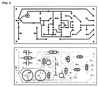
The zener diode VD2 limits the supply voltage to 15 V. The R5-C4-VD4 chain is used to set the RS-trigger on the elements DD1.2, DD1.3 to its initial state when power is applied (diode VD4 quickly discharges C4 when the network fails). At the moment the device is turned on, input 8 DD1.2 is low. For the logical element 2I-NOT, this level is switching. A feature of the RS flip-flop is that it fires from the first zero pulse, and does not respond to the rest. The integrating circuit R3-C3-VD3 creates a time delay when turned on (about 3 s). The charge of the capacitor C3 comes from the rectifier VD1 through the resistor R3 (the diode VD3 quickly discharges C3 in the event of a power failure). At the initial moment at the input 8 DD1.2 - low level, and at the input 13 DD1.3 - high. With this state of the input signals of the RS flip-flop, output 11 DD1.3 is low, and the transistor VT1 is closed. The DA1 chip is de-energized, the triac VS1 is turned off, and a current-limiting resistor R10 is connected in series with the load Rn. After charging the capacitor C4, a high level is set at pin 8 DD1.2. Single signals at both inputs of the RS flip-flop correspond to the information storage mode. After 3 s, "13" appears at input 1.3 DD0, the flip-flop flips and sends a high level to transistor VT1. The transistor opens and turns on the LED chip DA1. The microcircuit consists of an infrared emitting diode optically coupled to a two-way voltage zero crossing detector and a triac output circuit. The output circuit DA1 opens the triac VS1 (the pulsed output current of the microcircuit can reach 1 A, but this output cannot be loaded with a constant load). Thyristor VS1 opens, shunts the limiting resistor R10, and the full mains voltage is supplied to the load. In the event of a network failure, capacitor C4 is discharged through VD4, a low level is formed at input 8 DD1.2, and the trigger returns to its original state, i.e. a low level is applied to transistor VT1. The transistor closes, turns off the triac VS1, and the limiting resistor R10 is included in the load circuit. When the network appears and the exposure time (3 s) expires, the trigger switches, and the triac that turns on shunts the limiting resistor. The time delay can be corrected by changing the ratings of the R3-C3 chain. The device is made on a printed circuit board with dimensions of 91x41 mm (Fig. 2).
The resistance of the resistor R10 is selected based on the maximum allowable current of the protected device. Triac VS1 is selected according to the required operating current. It should be borne in mind that the currents switched by triacs depend on temperature. Therefore, triacs must be installed on radiators. Only one triac can be connected to one output of the DA1 chip. When checking the device, the mains voltage varied in the range from 120 to 270 V. If such a wide range is not needed, the capacitance of capacitor C1 can be halved. Author: V.Kalashnik, Voronezh
Machine for thinning flowers in gardens
02.05.2024 Advanced Infrared Microscope
02.05.2024 Air trap for insects
01.05.2024
▪ Created the most accurate scales in the world ▪ Artificial muscle made of crystalline plastic
▪ section of the site Electricity for beginners. Article selection ▪ article Flea market. Popular expression ▪ article Which bird migrates the greatest distances? Detailed answer ▪ article Technique of external heart massage. Health care ▪ article SMD transistors. Encyclopedia of radio electronics and electrical engineering
Home page | Library | Articles | Website map | Site Reviews
www.diagram.com.ua |


 Leave your comment on this article: