|
|


 Arabic
 Bengali
 Chinese
 English
 French
 German
 Hebrew
 Hindi
Hindi Italian
 Japanese
 Korean
 Malay
Malay Polish
 Portuguese
 Spanish
 Turkish
 Ukrainian
 Vietnamese
|
ENCYCLOPEDIA OF RADIO ELECTRONICS AND ELECTRICAL ENGINEERING Universal function generator. Encyclopedia of radio electronics and electrical engineering
Encyclopedia of radio electronics and electrical engineering / Measuring technology Introduction to a relatively simple function generator on the MAX038 microcircuit of the functions of frequency sweeping and a mark generator will make it possible to carry out a variety of measurements, adjustments and performance monitoring of various electronic equipment in a wide frequency range. The interesting possibilities of application that this generator has can be obtained by introducing similar nodes into other functional generators, the descriptions of which have been published in our journal in the last two or three years. When carrying out a number of measurements, a functional generator, along with a multimeter and an oscilloscope, is an indispensable device, which is perhaps included in the main necessary complex of a radio amateur's home laboratory. The oscillating frequency generator is also indispensable in the study, for example, of the amplitude-frequency characteristics. It allows you to observe the change in characteristics depending on the variation of the parameters of the circuits under study, while in some cases the tuning time of the resonant circuits can be tens or even hundreds of times less than in the classical method of studying the frequency response by points. Usually, in simple function generators with a small frequency range, there are no adjustments for the duty cycle of rectangular pulses, as well as for the forward and reverse steps of the sawtooth voltage, there is no possibility of obtaining a frequency or pulse-width modulated signal. As for swept frequency generators, they usually have a lot of resonant circuits, they are difficult to tune, and their manufacture is often beyond the power of medium-skilled radio amateurs. In simple GKCh [2], there are usually no signals of frequency marks, and therefore, without a frequency meter, there is very little sense from such devices. The generator offered to the attention of radio amateur designers is free from the listed shortcomings. Most of the device is assembled on digital microcircuits, which makes it as easy as possible to establish it. Even a radio amateur with little experience can make it. The description contains recommendations for changing some characteristics "to your taste". Main technical characteristics of the generator The operating frequency range is divided into nine sub-ranges: 1) 0,095 Hz...1,1 Hz; 2) 0,95 Hz... 11 Hz; 4) 95 Hz...1100 Hz; 5) 0,95 kHz...11 kHz; 6) 9,5 kHz...110 kHz; 7) 95 kHz...1100 kHz; 8) 0,95 MHz... 1 MHz; 9) 9 MHz...42 MHz*. Output signal shape - rectangular, sinusoidal, triangular, sawtooth. Peak-to-peak output voltage swing (at load resistance RH = 50 ohms) - 1 V. The duty cycle of rectangular pulses is 0,053 ... 19. Adjustment of the frequency and duty cycle of the output signal is mutually independent. Label signals can be set at intervals of 10 and 1 MHz, 100, 10 and 1 kHz, and 100 Hz. The maximum modulating frequency at the PWM and FM inputs is 2 MHz, the frequency deviation Fo (FM) by an external modulating signal is up to ±50%. The basis of the generator (its circuit is shown in Fig. 1) is the MAXIM chip MAX038, a detailed description of which is given in [1].
"Deviation" is in the lowest position according to the scheme. The shape of the generator output signal is determined by the logic levels at the inputs AO, A1 and depends on the position of the switch SA6. The influence of the instability of the control signals for the inputs AO and A1 on the overall instability of the generation frequency was noticed. To minimize this effect, capacitors C12, C13 are designed to reduce the level of interference and ripple of the power supply. The frequency of the generated signal depends on the capacitance CF connected to the output COSC (capacitors C1 - C8) of the voltage at the input SADJ and the current flowing into the input IIN. The choice of subrange is made by switch SA1. Smooth frequency adjustment within the subband occurs at the IIN input. The value of the current entering the input is determined by the resistance of resistors R12, R13, the gain of the op amp DA1.1 and the position of the variable resistor R 20 slider. For subranges 2 - 8, it is 21 ... 240 μA. When switching to the 9th subrange, the gain scale DA1.1 increases due to a decrease in the OOS (introduction of R19) and the current IIN increases to 160 ... 750 μA. This is necessary due to the limitation of the minimum allowable capacitance value CF to 20 pF. When switching to the first subrange, R17 is introduced, reducing the voltage drop across R20, R21 by ten times and reducing IIN to 2,1 ... 24 μA, respectively. Thus, for subranges 1 - 8, the overlap factor is 11, and when switching from one subrange to another, the output frequency changes 10 times, which allows using one graduated scale of smooth frequency change. For the ninth range, a separate scale is needed, it is more stretched, the overlap coefficient is about 4,7. For each specific instance of DA2, it is better to experimentally select the width of the ninth range according to the value of the cutoff frequency of the microcircuit generation. In any case, to expand, narrow or shift frequency ranges, you can use the formulas: Fmin-UminR9/[CFR' (R12+R13)]; Fmax UmaxR9/[CFR' (R12+R13)], where Umin= 5R21/(R20+R21), Umax= 5, R' = R18 - for subranges 1 - 8, R'= R19 - for subrange 9; CF= C1 ...C8 (for the corresponding subrange). The parameters presented in the formulas are measured respectively: F - in kilohertz, U - in volts, R - in ohms, C - in picofarads. It should be noted that for the first subrange, due to the introduction of the resistor R17, the values of Umin and Umax, substituted into the formulas for calculating the frequency, must be reduced ten times relative to the one obtained. Capacitors C10, C11 are designed to improve the stability of the constant control voltage supplied to the input 5 0U DA1.1. The relative frequency detuning (±50% of F0) is carried out by the resistor R4 (SA3 in the "F0" position). To obtain frequency-modulated oscillations, an external modulating signal is applied to the FM input and SA3 is transferred to the upper position according to the scheme (FM position). For pulse-width modulation, an appropriate PWM input is used; duty cycle is adjusted by resistor R2. The concept of “duty cycle” is used here somewhat conditionally, more precisely, it is a change in the ratio of the positive half-wave relative to the duration of the period in percent: for rectangular oscillations, this is really the duty cycle, but for triangular oscillations, this is the ratio of the forward and reverse stroke times (the signal changes from the “straight” saw to "reverse"), for a sinusoidal signal - change (distortion) of the waveform. The latter can be useful for minimizing the harmonic distortion of the generator by adjusting the shape of the sinusoid. The amplitude of the modulating signals for the FM and PWM inputs must be no more than ±2,3 V. Switches SA4, SA5 are designed to disable the duty cycle and frequency control at the DADJ and FADJ inputs of the DA2 chip, while the duty cycle is set to 2 (50%), and the frequency exactly corresponds to that set by resistor R20. The output signal comes from the OUT DA2 output through the resistor R44 to the "Generator 1 output" socket. The inputs COSC, DADJ, FADJ of the microcircuit are very sensitive to external interference, it is advisable to connect them to the switches with a shielded cable or place the generator unit in a shielded compartment. To control the output signal level, it is convenient to use an external attenuator connected between the generator output and the input of the device under study. The attenuator given in [2] can be recommended; it provides an attenuation range from 0 to 64 dB in 1 dB steps and is well matched in terms of input and output impedance. In the sweep mode, the input "√" of the generator is connected to the corresponding output of the oscilloscope. The frequency control of the GKCh synchronously with the sweep of the oscilloscope is performed at the input NN of the DA2 microcircuit. The signal from the input goes to the capacitor C9, where the constant component is cut off. Further, from the engine of the variable resistor R6, which regulates the amplitude of the control signal and, accordingly, the width of the oscillation bandwidth of the generator, it goes to the inverting amplifier-adder DA1.1. Summed up with a constant component that determines the center frequency of the swing and is regulated by resistor R20, the signal is fed to the UN DA2 input. Zener diode VD1 limits the maximum allowable current for input IIN to 750 uA. The frequency label generator consists of a master oscillator for DD1.1 - DD1.3, dividers for DD3 and DD4, a DD5.1 trigger and a comparator for DA1.4. The quartz master oscillator generates a signal with a frequency of 10 MHz, which is fed to the input of the divider DD3 (division ratio 10). Further, from the output of DD3, a signal of 1 MHz is fed to the input of a divider with a variable division ratio DD4. Depending on the position of the SA7.1 switch, at the input C of the DD5.1 trigger, there will be a signal with a frequency of 10 MHz, 1 MHz, or a signal whose frequency is determined by the division factor DD4. The inputs of the JK flip-flop receives a signal from the SYNC DA2 output, the frequency of which is equal to the frequency of the generator output signal, and the phase is shifted by 90 degrees. A low-pass filter is connected to the trigger output on the elements R40, C22-C27 (the cutoff frequency is determined by the position of SA8). Thus, at the input of the comparator DA1.4 we obtain low-frequency beats of the output frequency of the generator and frequencies that are multiples of the frequency at the clock input of DD5.1. The beat amplitude is the higher, the closer the above components are located along the frequency axis. Therefore, with a smooth change in the output frequency of the generator signal, bursts of the beat signal will be present at the input of DA1.4, indicating that the frequency of the output signal of the generator is a multiple of the frequency of the mark signal. The burst width (in time) depends on the bandwidth of the low-pass filter and is determined by the position of SA8, this is done to obtain clear marks at different spans and on different ranges of the generator. Resistor R36 determines the threshold of the comparator, cutting off beat noise below a given amplitude. The amplitude of the marks is regulated by resistor R46 and is added to the main signal at R45. The division factor DD4 is selected by the SA7.2 switch and allows you to get a signal at the output of the divider with frequencies of 100, 10, 1 kHz, 100 Hz. When SA7 is in the two extreme (upper according to the scheme) positions, DD4 performs a single count and stops - there is no signal at its output Q. To expand the capabilities of the generator, you can supplement the frequency grid of the tag signal with the necessary set of frequencies, for example, 465 kHz, to tune the IF of radio receivers. In this case, the division factor is chosen based on the formula: N \u1000d M (1R100 + 2R10 + 4RZ + P5) + PXNUMX, where N is the division factor; M - module, determined by the code for Ka, Kb, Ks; P1 - thousand multiplier, determined by the code on J2, J3, J4; Р2, РЗ, Р4 - multipliers of hundreds, tens, units, they are determined by the code on J13-J16, J9-J12, J5-J8; P5 - the remainder, which is determined by the code J1-J4. A detailed description of the operation of the K564IE15 chip is given in [3]. The generator has a separate "Mark" output, which can be useful in a number of measurements where it is necessary to have an exemplary quartz frequency. The auxiliary audio frequency generator on DA1.2 is assembled according to a typical scheme; it can be used to modulate the main generator in frequency or pulse width modulation, or as a separate generator. The detector (Fig. 2) is assembled according to the voltage doubling scheme and allows you to operate in the range of 10 kHz ... 50 MHz when using an oscilloscope sweep frequency of no more than 100 Hz.
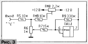
To study low-frequency circuits, the sweep frequency must be very low, the use of a conventional oscilloscope does not allow you to see the frequency response. With a storage oscilloscope, it is possible to observe the frequency characteristics starting from a frequency of 0,1 Hz. In this case, it is necessary to apply another input synchronization circuit, for example, shown in Fig. 3.
Also, for this purpose, it is better to make a separate detector head by increasing the capacitances of capacitors C1 and C2 (see Fig. 2). Increasing their capacitance expands the frequency range from below, while simultaneously reducing the allowable sweep frequency of the oscilloscope. To obtain labels at low frequencies, you must select the appropriate division factor DD4 and use a high-Q filter instead of a filter on R40, C22-C27; However, there is a limitation - it is difficult to isolate beats at low frequencies. The power supply (Fig. 4) is assembled according to the usual scheme and generates supply voltages of ±5 V and +12 V. Current consumption on the corresponding buses does not exceed the specified limits: +5 V - 300 mA; -5V-100mA;+12V-50mA; -12V-50mA.
The device uses MLT 0,125 resistors, it is allowed to use SP, SP0, SP4 as variables. Frequency-setting capacitors must have a small TKE - the KLS, KM-5 (C5-C8), K73-9, K73-16, K73-17 (C2-C4) series are applicable. Polar capacitor C1 - K52-1 with low leakage current; the rest of the capacitors - any. Switches SA1, SA6-SA8 - PG. Chips DD1 - DD3, DD5 are interchangeable with similar series K155, K555, K533, you just need to take into account the corresponding change in current consumption. Chip series 564 or K564 (DD4) will completely replace K561IE15. The printed circuit board for the generator was not developed. When placing elements and connections on the board, it is necessary to separate as far as possible all the circuits associated with the inputs (pins 3-10) of DA2 from the rest of the circuits. The generator setting begins with the selection of capacitors C1-C6, so that when switching ranges, the frequency changes exactly ten times. Capacitors C7, C8 are best selected after the final assembly of the structure, since the total capacitance CF for subranges 8,9 is affected by the capacitance of the connecting cable, mounting and other parasitic capacitances. After that, two scales for the resistor R20 are graduated (for subranges 1-8 and 9). Next, the shape of the output signal is checked depending on the position of SA6 and the limits of duty cycle control and detuning. The range of their adjustment can be changed by recalculating the divider R1-R4, taking into account that the voltages at the inputs FADJ and DADJ must be within ± 2,3 V. Then, a signal from the oscilloscope is applied to the "√" input, the Y input of the oscilloscope is connected to the output 7 DA1.1, the slider of the resistor R20 is set to the middle of one of the sub-ranges, R6 is placed in the upper position according to the scheme and by selecting R5 they ensure that the signal at pin 7 DA1.1 is within 0,2 ... 7,5 V. This corresponds to the maximum swing band. Inside the band, the frequency can change by a factor of 300; to reduce this value, the resistance R5 is increased to the required value. The setting of the frequency mark generator begins with setting the frequency of the master oscillator. The frequency meter is connected to pin 6 of DD1.3 and by adjusting the capacitor C18 the frequency is set to 10 MHz. Next, check the correspondence of the frequencies at the output of the frequencies of the tags to the positions of the switch SA7. After that, the presence of a beat signal at pin 13 of DA1.4 is checked and the comparator threshold is set with resistor R36 until clear narrow marks are obtained at the output of DA1.4. On this setting of the generator can be considered complete. The auxiliary audio frequency generator on DA1.2 (see Fig. 1) is tuned by tuning R23 until a stable generation of a sinusoidal signal is obtained. Setting up the power supply consists in setting the appropriate output voltages using resistors R1, R4, R6. To study the frequency response, the installation is assembled according to the scheme in Fig. 5.
Switch SA6 is moved to the position of generating a sinusoidal signal. The proposed location of the frequency response is set by the switch SA1 and the resistor R20, the required swing band (review) is set by the resistor R6. Using the SA7 switch, the necessary frequency marks are selected. The SA8 switch is used to achieve clear, stable marks on the oscilloscope screen. By changing the parameters of the device under study, the change in the characteristic points of the frequency response is monitored: in frequency - relative to the marks, in amplitude - relative to the positions of the attenuator. *The upper frequency of the ninth subband is determined by a specific instance of the MAX038 microcircuit: its typical value is about 40 MHz, the minimum is 20 MHz. Literature
Author: A.Matykin, Moscow
Artificial leather for touch emulation
15.04.2024 Petgugu Global cat litter
15.04.2024 The attractiveness of caring men
14.04.2024
▪ Contacts between shipbuilders of ancient Rome and Vietnam ▪ Hearing does not deteriorate with age ▪ Autonomous fighting robots of the Pentagon
▪ section of the site Sites of amateur radio equipment. Article selection ▪ article Advertising and promotional activities. Lecture notes ▪ article The simplest sailing boat. Personal transport ▪ article Chain with a break. Focus Secret
Home page | Library | Articles | Website map | Site Reviews
www.diagram.com.ua |


 Leave your comment on this article: