|
|


 Arabic
 Bengali
 Chinese
 English
 French
 German
 Hebrew
 Hindi
Hindi Italian
 Japanese
 Korean
 Malay
Malay Polish
 Portuguese
 Spanish
 Turkish
 Ukrainian
 Vietnamese
|
ENCYCLOPEDIA OF RADIO ELECTRONICS AND ELECTRICAL ENGINEERING Triac dimmer. Encyclopedia of radio electronics and electrical engineering
Encyclopedia of radio electronics and electrical engineering / Lighting The dimmer switch offered to the attention of readers allows you to adjust the brightness of lighting in the premises, the power of household heating elements, the speed of rotation of AC motors. It can also be used to reduce the starting current of incandescent lamps, which prolongs their service life. The dimmer is controlled by buttons, which makes it possible to turn the load on and off at a noticeable distance from the controlled object. And so that the button can be easily found in the dark, an LED is installed next to it, which glows only when the light is off. This regulator is made on the basis of the device described in the article by S. Biryukov "Timistor power regulators" ("Radio", 1996, No. 1, pp. 44 - 46). In contrast, the dimmer proposed in this article is not completely disconnected from the network, which required it to be finalized in order to reduce the current consumption. As a result, the current dropped to 1,5 mA in all modes of operation. After refinement, the range of power control has also expanded. With a hundred-watt load, it is about 99%. Schematic diagram of the dimmer is shown in fig. 1. To control the VS1 triac, a short pulse shaper is required, one of the outputs of which is connected to the mains wire. The shaper is powered from a source assembled on the elements C2, R2, VD1 - VD3, C4, C5. Diodes VD1, VD2 perform the functions of a rectifier. The rectified voltage is stabilized at 10 V by the Zener diode VD3. Capacitors C4, C5 are part of the smoothing filter, and C4 shunts mainly high-frequency mains interference, which are not suppressed by the oxide capacitor C5 due to its significant parasitic inductance.
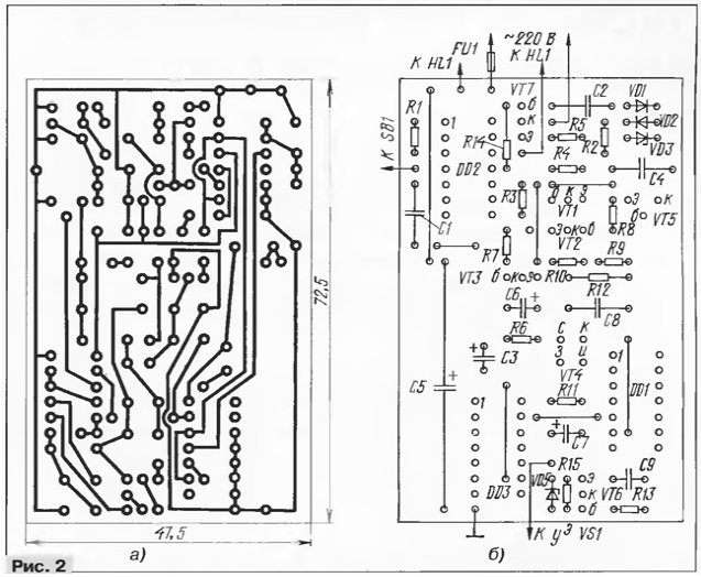
With a positive voltage at the anode, most triacs can be opened by pulses of any (relative to the cathode) polarity arriving at the control electrode, and with a negative voltage, by pulses of only negative polarity. The positive output of the power supply of the described regulator is connected to the triac cathode. As a result, negative pulses will be formed on its control electrode for any polarity at the anode. When using the phase-pulse method, the power in the load is regulated by changing the part of the half-cycle of the mains voltage, during which the triac passes current. To do this, it is necessary to select the beginning of each half-cycle of the mains voltage (it corresponds to a voltage equal to or close to zero), and then for 10 ms (the duration of half a period of the mains voltage with a frequency of 50 Hz) to form the control pulse itself. Thus, the sooner the triac opens, the more power will be allocated to the load. The pulse shaper with a frequency of 100 Hz is assembled on the elements VT1, VT2, R4, R5, R8. During the positive half-cycle of the mains voltage, the transistor VT1 is open, during the negative half-cycle, the transistor VT2. Resistor R5 limits the base current of the transistors. Resistor R8 performs the functions of the collector load of both transistors. When the mains voltage is close to zero, both transistors are closed and the voltage at their collectors is equal to the voltage at the negative terminal of the power supply. At the same time, short pulses of negative polarity are formed at input 1 of the DD1.1 element, corresponding to the beginning of each half-cycle of the mains voltage. In the on state of the regulator, at input 2 of the DD1.1 element, there is a voltage corresponding to a high logic level, therefore, negative pulses at input 1 of this element are inverted by it and fed to the base of the transistor VT5, which is connected according to the emitter follower circuit. The current flowing through it charges the capacitor C8 almost to the voltage of the power supply. The capacitor is discharged through the circuit R9, R10, R12, VT4. When it is discharged to a voltage corresponding to the threshold, the elements DD1.2 and DD1.3 are switched. The voltage drop that occurs at the output 11 of the DD1.3 element is differentiated by the C9R13 circuit and, in the form of a pulse with a duration of about 12 μs, is fed through the DD1.4 inverter to the current amplifier on the VT6 transistor, and then to the control electrode of the triac VS1. The variable resistor R10 regulates the duration of the discharge of the capacitor C8, which determines the moment the triac is turned on, and hence the effective voltage at the load. The VD5 zener diode provides a reliable start of the dimming device. In its absence, at the first moment the regulator is turned on after a break in operation, a current begins to flow through the control transition of the triac and transistor VT6, which does not allow the filter capacitor C5 to charge and prevents the power supply voltage from rising to the nominal value. Resistor R15 limits the current through the control transition of the triac. The need for such a limitation is not caused by ensuring the safety of the operation of the zener diode and triac (such a short current pulse cannot disable them), but by a possible deterioration in the efficiency of the dimmer. On the inverter DD2.1 and the trigger DD3.1, a control device for turning the dimmer on and off is assembled, on the transistor VT4 - a node for smooth switching on the load, and on elements DD2.2, DD2.3, VT7, HL1 - a node for backlighting the button SB1 (SB2 - SBn ). When the regulator is initially turned on or after a power failure, the C3R3 circuit generates a positive pulse at the R input of the DD3.1 trigger, setting it to the zero state, at which the load is turned off. Element DD3.1 responds to a positive voltage drop at input C and changes its state to the opposite each time it appears. The R1C1 chain suppresses the bounce of the contacts of the SB1 button. Through the resistor R1 also sets the voltage at the input of the inverter DD2.1. When you press the SB1 button, a positive voltage drop occurs at the output of this element, switching the trigger DD3.1 to a single state. A high logic level, which appears at the same time at the direct output of the trigger, allows the operation of the logic element DD1.1. At the same time, through the resistor R6, the capacitor C6 is charged to almost 10 V. As the voltage across this capacitor increases, the voltage at the gate of the transistor VT4 increases and the resistance of its channel gradually decreases, reaching a minimum 5 ... 7 s after the start of charging the capacitor C6. And since the channel of the transistor VT4 in series with the resistor R10 is included in the discharge circuit of the capacitor C8, the power in the load gradually increases to the level set by the resistor R10. Resistor R11 creates a minimum negative bias at the gate of transistor VT4, which ensures that the dimmer switch is completely turned off at zero resistance of resistor R10. This offset is also necessary so that when the dimmer is turned on, the load immediately turns on. Capacitor C7 shunts resistor R11 in alternating voltage, excluding it from the discharge circuit of capacitor C8. A low voltage level from the inverse input of the trigger DD3.1 closes the transistor VT3 and prohibits the switching of inverters DD2.2 and DD2.3. As a result, the transistor VT7 remains closed, no current flows through it, and the HL1 LED included in its emitter circuit does not light up. The next time you press the SB1 (SB2-SBn) button, the trigger switches back to the zero state. A logical zero from its output 13 prohibits the switching of the element DD1.1, and a high logic level is set at the output of the latter, maintaining the open state of the transistor VT5. As a result, the capacitor C8 will be charged to the maximum voltage, and the load is de-energized. The logic zero level present at this time at the output 12 of the trigger will open the transistor VT3, through which the capacitor C6 will quickly discharge, and the dimmer will be ready for a new switch on. A high logic voltage level from the output 12 of the trigger will also go to the inputs 13 and 9 of the logic elements DD2.2, DD2.3 and will allow them to skip negative pulses from the load of transistors VT1, VT2. These pulses will open the transistor VT7 for a short time, and the HL1 LED included in its emitter circuit will light up. Resistor R14 limits the average current through the LED so as not to overload the power supply, otherwise its voltage will begin to drop. All parts of the dimmer, except for the triac VS1 and the LED HL1, are mounted on a printed circuit board made of one-sided foil fiberglass. The board drawing is shown in fig. 2, a, and the location of the parts on it - in Fig. 2, b.
During installation, you can use fixed resistors C2 - ZZN or MLT and any variable resistor indicated on the resistance circuit diagram. Capacitors C1, C2, C8 - K73-15, K77 - 3 and others from the K70 - K78 series, capacitor C2 must be rated for a voltage of at least 250 V. Capacitor C3 - any oxide, C4, C9 - ceramic KM - 5, K10 - 17, C5 - K50 - 24 or K50 - 29, C6, C7 - K53 - 14. KD510, KD509 with any letter index can work in place of diodes. Zener diode VD3 - any with a stabilization voltage of 10 V. Transistors VT1, VT2 can be any low-power silicon pnp structures with a current transfer coefficient of more than 100. Transistors VT3, VT6, VT7 - low-power silicon, VT5 - KT201 series with any letter index. Silicon low-power transistors of the npn structure are also suitable, but in this case, you need to include a VD4 diode in the device, shown in the diagram with a dashed line. The diode protects the emitter junction from breakdown by a reverse voltage that appears on it every time after the VT5 transistor is closed. Field-effect transistor from the KP305 series with any letter index. Fuse FU1 must be rated for a current not less than the load current. Establishing a dimmer is reduced to the selection of a resistor R11. First of all, break the circuit connecting pin 2 of the element DD1.1 and pin 13 of the trigger DD3.1. Then pin 2 of DD1.1 is connected to its pin 1. After that, the slider of the resistor R10 is set to the lower position according to the diagram. In place of the resistor R11, a variable resistor with a resistance of 100 kOhm is included, and its slider is set in such a position that the resistance included in the circuit is zero. Next, turn on the dimmer to the network and wait until the nominal voltage of 10 V is established at the output of the power source. Then, using an oscilloscope to control the shape of the current pulses in the load, increase the resistance of the variable resistor (R11) until the triac VS1 stops opening. After that, the load is turned on and off several times, each time checking whether the transistor VT4 reliably closes the triac VS1. Then the variable resistor is replaced by a constant one and the connection of output 2 of the DD1.1 element with output 13 of the trigger DD3.1 is restored. If desired, by installing and selecting the resistor R12, it is possible to ensure that the maximum resistance of the resistor R10, operating as a rheostat, corresponds to zero voltage at the load. In order for the triac to drop as little voltage as possible when the load is fully turned on, it must open as quickly as possible after the start of the half-cycle. To do this, the mains voltage zero crossing pulse shaper must generate sufficiently short pulses. Their minimization is achieved by selecting resistors R4 and R8. It is undesirable to reduce the resistance of the resistor R5, TVK, as this will increase the power consumption. The dimmer has such a good feature: if the load was turned on, then after a short-term power failure in the network (for a period of no more than 2 minutes), it will turn on again. This is because capacitor C5 in the power supply filter discharges very slowly so that no logic gate is switched. When setting up a dimmer and its practical use, it should be remembered that all its elements, including the variable resistor axis, are under mains voltage. To limit the current through the HL1 LED, it is advisable to transfer the resistor R14 from the base circuit of the transistor VT7 to its emitter circuit, reducing the resistance R14 to 0,5 ... 1 kOhm. Author: A.Rudenko, Kharkov, Ukraine
Machine for thinning flowers in gardens
02.05.2024 Advanced Infrared Microscope
02.05.2024 Air trap for insects
01.05.2024
▪ Satellites will fly in a mirror pair ▪ CC2591 - high frequency amplifier chip ▪ Quantum dots - lamps of the future ▪ Quantum computers for data processing
▪ site section Power supplies. Article selection ▪ article by John Ray. Famous aphorisms ▪ article Who Was the First American President? Detailed answer ▪ article Insurance agent. Job description
Home page | Library | Articles | Website map | Site Reviews
www.diagram.com.ua |


 Leave your comment on this article: